ZR36015 Просмотр технического описания (PDF) - Unspecified
Номер в каталоге
Компоненты Описание
Список матч
ZR36015 Datasheet PDF : 27 Pages
| |||
PRELIMINARY
ZR36015
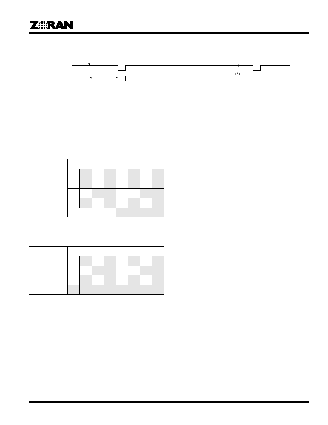
SYSCLKs before the trailing edge of VEN, then the following VEN signal (active high) will be ignored, and the VEN pulse after that
will be processed.
VEN
Line
BSY (signal)
BSY (bit)
GO
At least
3 SYSCLKS
VDelay
VWidth
Delay of Internal Processing
Figure 10. Relationship of BSY Terminal and BSY Flag and GO Bit
DECIMATION
Horizontal Decimation of data by a factor of 2 is supported for the ZR36015. This allows for the reduction of the volume of data being
stored in the Strip Buffer (and sent out over the BDATA bus) by half.
The tables below shows how data is decimated for each mode.
Decimation
Mode 0 (4:0:0)
Mode 1 (4:2:2)
Mode 3 (4:1:1)
Pixel Elements
Y0 Y1 Y2 Y3 Y4 Y5 Y6 Y7
Y0 Y1 Y2 Y3 Y4 Y5 Y6 Y7
U0 V0 U2 V2 U4 V4 U6 V6
Y0 Y1 Y2 Y3 Y4 Y5 Y6 Y7
U0/V0
U4/V4
During expansion there is no interpolation mode for the data (except as described below for mode 2).
In mode 2, the data is decimated horizontally as shown above for mode 1. But in addition, the UV data for every other line (starting
with the second line) is dropped. The figure below shows this case.
Decimation
Mode 2
(1st line)
Mode 2
(2nd line)
Pixel Elements
Y0 Y1 Y2 Y3 Y4 Y5 Y6 Y7
U0 V0 U2 V2 U4 V4 U6 V6
Y0 Y1 Y2 Y3 Y4 Y5 Y6 Y7
U0 V0 U2 V2 U4 V4 U6 V6
During Expansion in mode 2, the UV data for the 1st line is replicated to replace to corresponding UV data for the second line.
Note that the MCU for mode 2 will be H=2, V=2.
Sub-Buffer and Strip Buffer Interface
Figure 12 shows the Sub-Buffer Interfaces between the Pixel Data, the Coder Data, and the double buffered Strip Memory.
The Strip Memory Interface can perform a 16-bit read or write on every SYSCLK cycle. In order to keep up with the required data
throughput, the Pixel Data and Coder Data Sub-Buffers each must be able to perform a 16-bit read or write to the Strip Memory on
every other SYSCLK cycle. Therefore the Strip Memory Interface is shared between the Pixel Data, and Coder Data Sub-Buffers,
with each Sub-Buffer accessing the Strip Memory on alternate SYSCLK cycles. Figure TBD shows the timing for alternate read and
writes to the Strip Memory.
The Pixel Data Sub-Buffer performs conversion of the data between the PXDATA Bus and the Strip Memories. (The A Memory stores
the data for all the even pixels, and the B Memory stores the data for all the odd pixels; (see the section on Strip Memory Format).
9
Share Link: 