ZR36015 Просмотр технического описания (PDF) - Unspecified
Номер в каталоге
Компоненты Описание
Список матч
ZR36015 Datasheet PDF : 27 Pages
| |||
PRELIMINARY
ZR36015
Table 4: PXDATA Bus Sync Clock Frequency
MOD (1:0)
Pixel Side Coder Side
Format
Format
PXDATA Bus Sync
Clock Freq.1
0 (00)
(1:0:0)
(1:0:0)
SYSCLK
1 (01)
(4:2:2)
(4:2:2)
SYSCLK÷2
2 (10)
(4:2:2)
(4:1:1)
SYSCLK÷2
3 (11)
(4:1:1)
(4:1:1)
SYSCLK÷2
1. The sync clock freq. of the coder bus side is SYSCLK in all modes.
The data seen on the Pixel Bus during Compressoin is shown in
Figure 5.
unknown number of lines. At the end of processing, the “Number
of Lines” register will contain the number of lines that have been
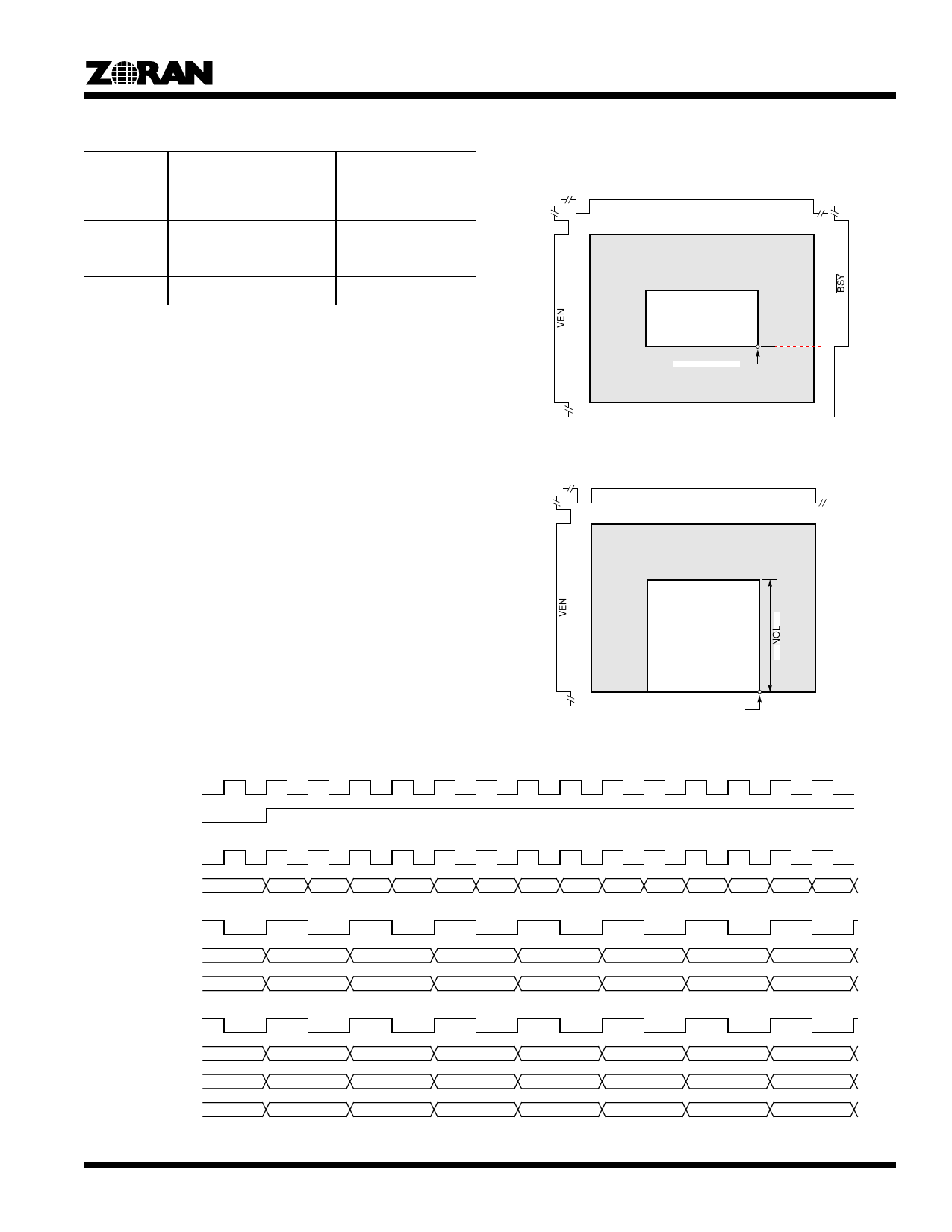
processed. Figure 7 illustrates the “active image area” for this
special case.
HEN
Active Image
Area
EOS Output
PIXEL PROCESSING TIMING
The leading edge of the frame is identified by the fall of VEN
(after the GO bit is set). Tge VDelay is counted from the follow-
ing rise of the VEN input. The HDelay is counted from the rise of
the HEN input. The HEN and VEN signals must remain high at
least until the end of the active image area (as defined by the
Configuration Register table).
HEN must conform to either A or B in Figure 8.
Within the image area defined by the VEN and HEN signals, is
the “Active Image Area”, which is determined by the HDelay,
HWidth, VDelay, and VWidth values in the configuration table.
Pixel processing is performed only on those pixels which lie in
the active image area defined in Figure 4. The width and height
of the active image area are determined by the “HWidth” and
“VHeight” values in the configuration register table.
If VWidth is set to zero (a special case), then lines will continue
to be processed for as long as VEN remains high (maximum of
8K lines). This feature allows processing of frames with an
Figure 6. Pixel Processing Image Area
HEN
Active Image
Area
EOS Output
Figure 7. EOS Asertion
SYSCLK
HEN
MOD[1:0] = 0
CLKCSC
PXDATA (15:8)
MOD[1:0] = 1, 2
CLKCSC
PXDATA (15:8)
PXDATA (7:0)
MOD[1:0] = 3
CLKCSC
PXDATA (15:8)
PXDATA (7:6)
PXDATA (5:4)
Y1
Y2
Y3
Y4
Y5
Y6
Y7
Y8
Y9
Y10
Y11
Y12
Y13
Y14
Y1
Y2
Y3
Y4
Y5
Y6
Y7
U1
V1
U2
V2
U3
V3
U4
Y1
Y2
Y3
Y4
Y5
Y6
Y7
U11
U12
U13
U14
U21
U22
U23
V11
V12
V13
V14
V21
V22
V23
Figure 5. Functional Timing Chart - Pixel Bus Side
7
Share Link: 