ZR36015 Просмотр технического описания (PDF) - Unspecified
Номер в каталоге
Компоненты Описание
Список матч
ZR36015 Datasheet PDF : 27 Pages
| |||
PRELIMINARY
ZR36015
The MOD(1:0) bits in the Mode Register determine the format of
the data on the PXDATA bus, and the DCM bit determines if
decimation is performed.
After the last of the data in the “Active Image Area” has been
converted to Block format and transferred to the Coder (as indi-
cated by the EOS output), the GO bit and the BSY bit (and BSY
signal) are cleared and the ZR36015 enters the IDLE state.
In order to compress a sequene of images, the GO bit must be
set for each image. However, the table values do not have to be
re-initialized for each image.
Expansion
When the GO bit is set to “1”, and the EDC bit equals “0”, then
the ZR36015 enters the Expansion State.
Setting the GO bit results in the BSY bit in the mode register
being set.
Once the GO bit is set, then on the falling edge of the Verticle
Sync Signal (VEN), the BSY output signal will be set. The BSY
bit (and output signl) will stay set until the end of the Expansion
process. The, to determine when the Expansion process has
completed. Note that the GO bit must be set at least three
SYSCLK cycles before the VEN goes from High to Low (see
figure ???).
Following the above, the ZR36015 monitores the VEN input to
detect the transition of VEN from low to high. This indicates the
beginning of the time interval when the image is to be output to
the PIXEL bus. The ZR36015 waits VDelay lines before putting
the first line of decoded data out to the PIXDATA bus.
The HEN input synchronized the line by line transfers of data to
the PXDATA bus. On the rise of HEN, the ZR36015 waits
HDelay SYSCLKs until outputting the decoded line of pixels
(HWIDTH of them) on the PXDATA bus.
The MOD(1:0) bits in the Mode Register and the data in the Con-
figuretino Tables, must match the format and size fo the data
being decodced by the ZR36050.
The DCM bit is not used in expansion.
After the last of the data in the “Active Image Area” has been
transmitted to the PXDATA bus, the GO bit and the BSY bit (and
BSY signal) are cleared, and the ZR36015 enters the IDLE
state.
In order to expand a sequence of images, the GO bit must be set
for each image. However, the table values do not have to be re-
initialized for each image.
PXDATA bus. Once host access is selected, the WE and RD
signals initiate the writing and reading of data (using the
PXDATA bus), to locations specified by the ADD(1:0) inputs.
Since the Host and image source share PXDATA(7:0), an
external bidirectional buffer is required on PXDATA(7:0) in order
to avoid bus contention. The ADD(1:0), RD, and WR inputs are
ignored when Host Access is not selected by SPH. The table
below shows the addressing of the internal control registers by
the ADD(1:0) address inputs.
Pixel Bus Formats
The Pixel Bus “PXDATA(15:0), is divided into two bytes.
PXDATA(15:8) is always used to represent the Y data, while
PXDATA(7:0) is always used to represent the UV data.
The data formats of PXDATA are according to the setting of the
MOD(1:0) bits in the Mode Register.
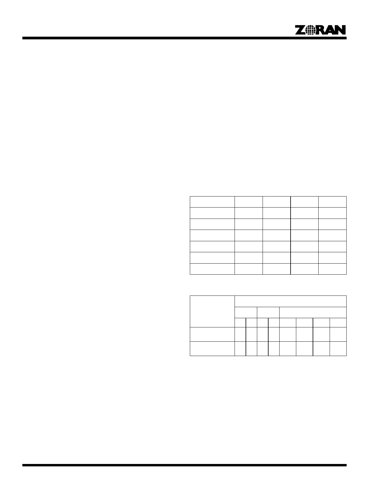
Table 2 and 3 show the format of PXDATA bus for each mode.
Table 2: Pixel Bus Data Format (Mode 3)
PXDATA
1st
2nd
3rd
4th
PXDATA (15:8)
Y1 (7:0) Y1 (7:0) Y1 (7:0) Y1 (7:)
PXDATA (7)
U1 (7)
U1 (5)
U1 (3)
U1 (1)
PXDATA (6)
U1 (6)
U1 (4)
U1 (2)
U1 (0)
PXDATA (5)
V1 (7)
V1 (5)
V1 (3)
V1 (1)
PXDATA (4)
V1 (6)
V1 (4)
V1 (2)
V1 (0)
PXDATA (3:0)
–
–
–
–
Table 3: Pixel Bus Data Format (Modes 0, 1, 3)
Format
PXDATA
PXDATA (15:8)
(Y)
PXDATA (7:0)
(UV)
(1:0:0) (4:2:2)
(4:1:1)
1st 2nd 1st 2nd
1st
2nd
3rd
4th
Y0 Y1 Y0 Y1
Y0
Y1
Y2
Y3
–
–
U0 V0 U0 (7:6) U0 (5:4) U0 (3:2) U0 (1:0)
V0 (7:6) V0 (5:4) V0 (3:2) V0 (1:0)
PXDATA Syncronization Clock Frequency:
The input and output of data on PXDATA(15:0) are carried out
in synchronization with the clock signal of SYSCLK for mode 0,
or SYSCLK/2 for modes 1, 2 and 3. Table 4 shows the PXDATA
bus sync clock frequency for each of the modes of operation.
System Interface
The SPH input is used to select host access to the ZR36015,
(set SPH to ‘1’). Host access for read/write of the ZR36015’s
control registers is carried out using the system interface pins
(RD,WR, and ADD(1:0)), in addition to the lower 8-bits of
6
Share Link: 