AD650KP Просмотр технического описания (PDF) - Analog Devices
Номер в каталоге
Компоненты Описание
Список матч
AD650KP Datasheet PDF : 12 Pages
| |||
AD650
OTHER CIRCUIT CONSIDERATIONS
The input amplifier connected to Pins 1, 2 and 3 is not a standard
operational amplifier. Rather, the design has been optimized for
simplicity and high speed. The single largest difference between
this amplifier and a normal op amp is the lack of an integrator
(or level shift) stage. Consequently the voltage on the output
(Pin 1) must always be more positive than 2 volts below the
inputs (Pins 2 and 3). For example, in the F-to-V conversion
mode, see Figure 6, the noninverting input of the op amp (Pin 2) is
grounded, which means that the output (Pin 1) will not be able
to go below –2 volts. Normal operation of the circuit as shown
in the figure will never call for a negative voltage at the output
but one may imagine an arrangement calling for a bipolar out-
put voltage (say ± 10 volts) by connecting an extra resistor from
Pin 3 to a positive voltage. This will not work.
Care should be taken under conditions where a high positive
input voltage exists at or before power up. These situations can
cause a latch up at the integrator output (Pin 1). This is a non-
destructive latch and, as such, normal operation can be restored
by cycling the power supply. Latch up can be prevented by
connecting two diodes (e.g., 1N914 or 1N4148) as shown in
Figure 4, thereby, preventing Pin 1 from swinging below Pin 2.
A second major difference is that the output will only sink 1 mA
to the negative supply. There is no pulldown stage at the output
other than the 1 mA current source used for the V-to-F conver-
sion. The op amp will source a great deal of current from the
positive supply, and it is internally protected by current limiting.
The output of the op amp may be driven to within 3 volts of the
positive supply when it is not sourcing external current. When
sourcing 10 mA the output voltage may be driven to within
6 volts of the positive supply.
A third difference between this op amp and a normal device is
that the inverting input, Pin 3, is bias current compensated and
the noninverting input is not bias current compensated. The
bias current at the inverting input is nominally zero, but may be
as much as 20 nA in either direction. The noninverting input
typically has a bias current of 40 nA that always flows into the
node (an npn input transistor). Therefore, it is not possible to
match input voltage drops due to bias currents by matching
input resistors.
The op amp has provisions for trimming the input offset volt-
age. A potentiometer of 20 kΩ is connected to Pins 13 and 14
and the wiper is connected to the positive supply through a
250 kΩ resistor. A potential of about 0.6 volt is established
across the 250 kΩ resistor, and the 3 µA current is injected into
the null pins. It is also possible to null the op amp offset voltage
by using only one of the null pins and use a bipolar current
either into or out of the null pin. The amount of current re-
quired will be very small—typically less than 3 µA. This tech-
nique is shown in the applications section of this data sheet: the
auto-zero circuit uses this technique.
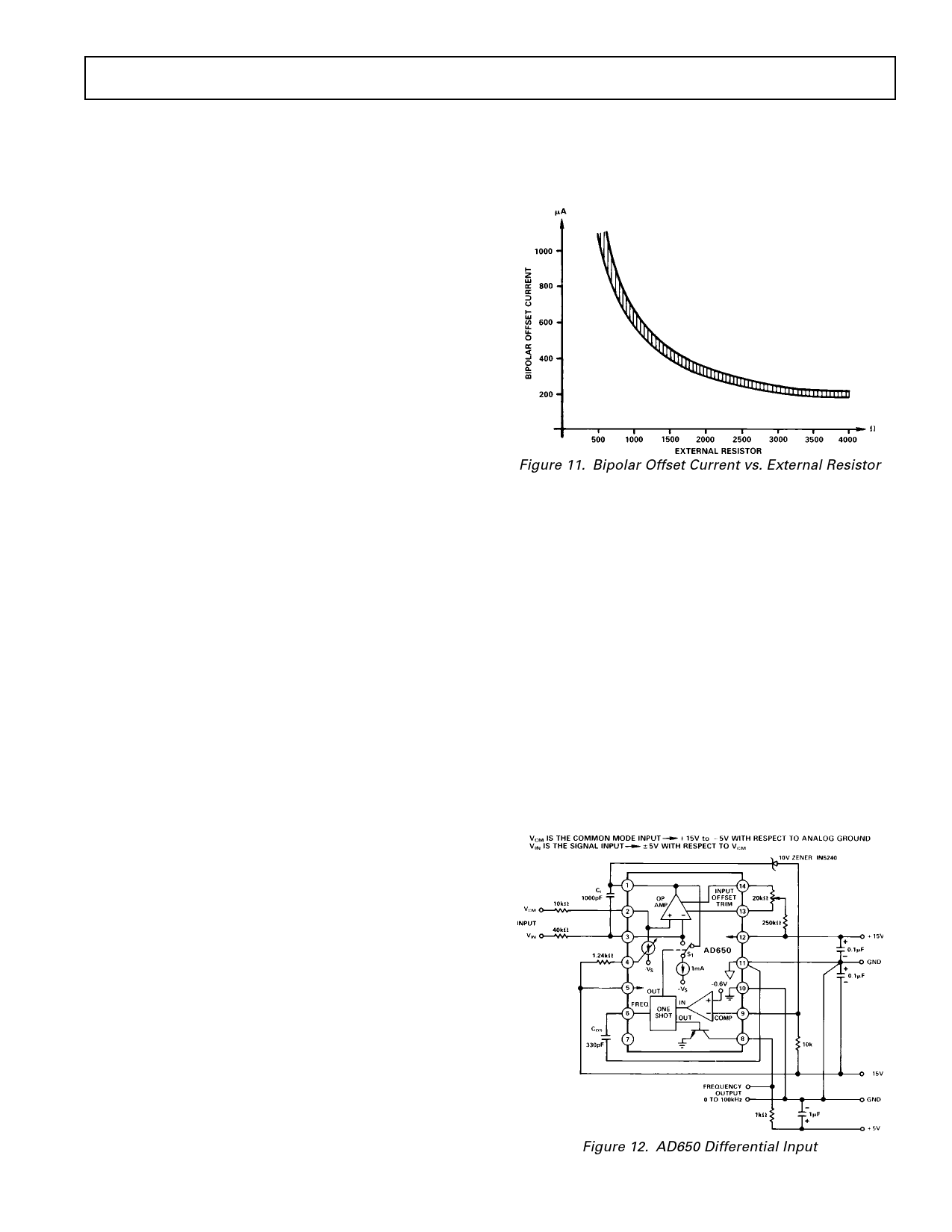
The bipolar offset current is activated by connecting a 1.24 kΩ
resistor between Pin 4 and the negative supply. The resultant
current delivered to the op amp noninverting input is nominally
0.5 mA and has a tolerance of ± 10%. This current is then used
to provide an offset voltage when Pin 2 is tied to ground
through a resistor. The 0.5 mA which appears at Pin 2 is also
flowing through the 1.24 kΩ resistor and this current may be by
observing the voltage across the 1.24 kΩ resistor. An external re-
sistor is used to activate the bipolar offset current source to pro-
vide the lowest tolerance and temperature drift of the resultant
offset voltage. It is possible to use other values of resistance
between Pin 4 and –VS to obtain a bipolar offset current differ-
ent than 0.5 mA. Figure 11 is a graph of the relationship be-
tween the bipolar offset current and the value of the resistor
used to activate the source.
Figure 11. Bipolar Offset Current vs. External Resistor
APPLICATIONS
DIFFERENTIAL VOLTAGE-TO-FREQUENCY
CONVERSION
The circuit of Figure 12 accepts a true floating differential input
signal. The common-mode input, VCM, may be in the range
+15 to –5 volts with respect to analog ground. The signal input,
VIN, may be ± 5 volts with respect to the common-mode input.
Both inputs are low impedance: the source which drives the
common-mode input must supply the 0.5 mA drawn by the
bipolar offset current source and the source which drives the
signal input must supply the integration current.
If less common-mode voltage range is required, a lower voltage
Zener may be used. For example, if a 5 volt Zener is used, the
VCM input may be in the range +10 to –5 volt. If the Zener is
not used at all, the common-mode range will be ± 5 volts with
respect to analog ground. If no Zener is used, the 10k pulldown
resistor is not needed and the integrator output (Pin 1) is con-
nected directly to the comparator input (Pin 9).
Figure 12. AD650 Differential Input
REV. A
–9–
Share Link: 