AD650KP Просмотр технического описания (PDF) - Analog Devices
Номер в каталоге
Компоненты Описание
Список матч
AD650KP Datasheet PDF : 12 Pages
| |||
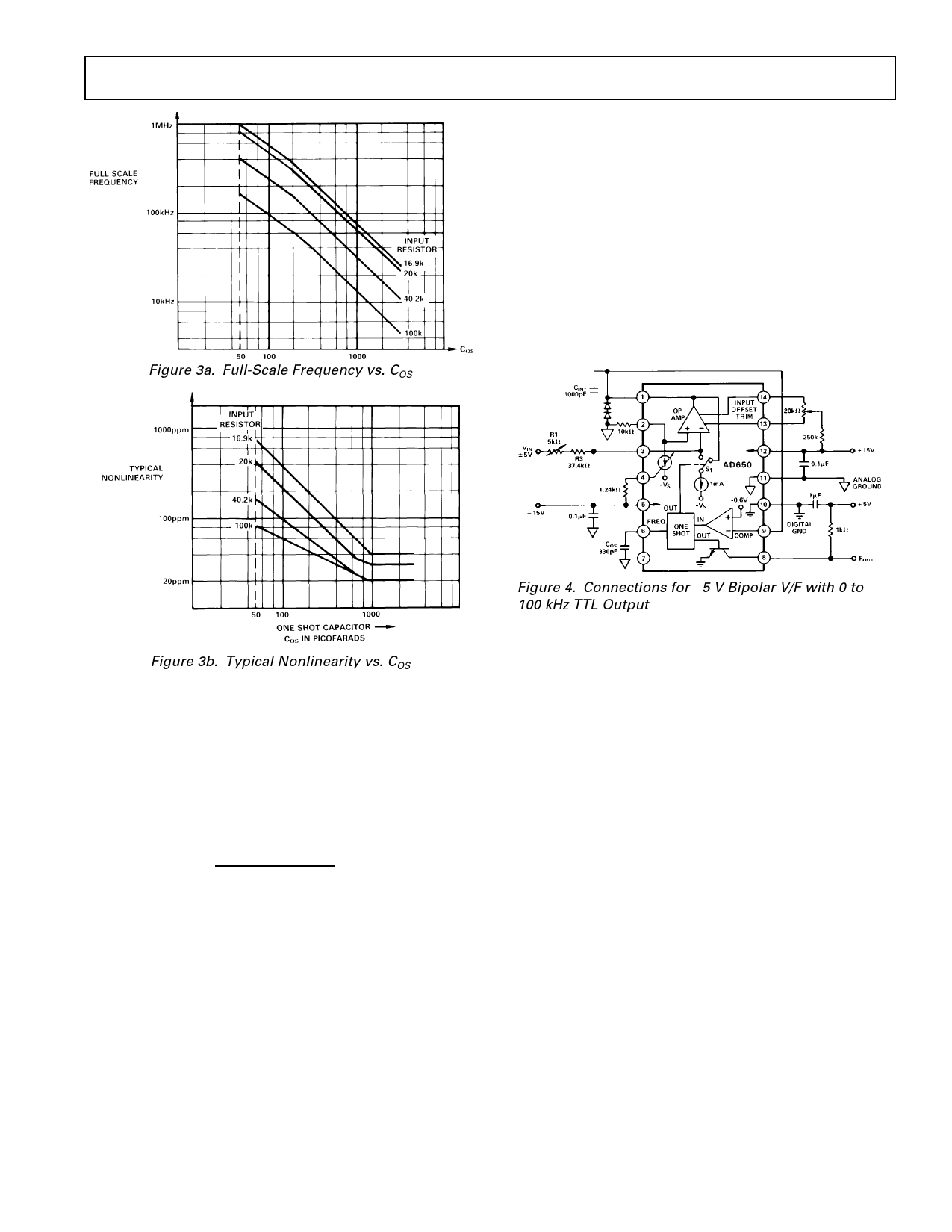
Figure 3a. Full-Scale Frequency vs. COS
AD650
BIPOLAR V/F
Figure 4 shows how the internal bipolar current sink is used to
provide a half-scale offset for a ± 5 V signal range, while provid-
ing a 100 kHz maximum output frequency. The nominally 0.5 mA
(± 10%) offset current sink is enabled when a 1.24 kΩ resistor is
connected between Pins 4 and 5. Thus, with the grounded 10 kΩ
nominal resistance shown, a –5 V offset is developed at Pin 2.
Since Pin 3 must also be at –5 V, the current through RIN is
10 V/40 kΩ = +0.25 mA at VIN = +5 V, and 0 mA at
VIN = –5 V.
Components are selected using the same guidelines outlined for
the unipolar configuration with one alteration. The voltage
across the total signal range must be equated to the maximum
Figure 4. Connections for ±5 V Bipolar V/F with 0 to
100 kHz TTL Output
Figure 3b. Typical Nonlinearity vs. COS
can be rejected. If the output frequency is measured by counting
pulses during a constant gate period, the integration provides
infinite normal-mode rejection for frequencies corresponding to
the gate period and its harmonics. However, if the integrator
stage becomes saturated by an excessively large noise pulse, the
continuous integration of the signal will be interrupted, allowing
the noise to appear at the output. If the approximate amount of
noise that will appear on CINT is known (VNOISE), the value of
CINT can be checked using the following inequality:
CINT
>
tOS ×1×10⁻³ A
+V S – 3V –V NOISE
(8)
For example, consider an application calling for a maximum
frequency of 75 kHz, a 0 volt–1 volt signal range, and supply
voltages of only ± 9 volts. The component selection guide of Fig-
ure 3 is used to select 2.0 kΩ for RIN and 1000 pF for COS. This
results in a one shot time period of approximately 7 µs. Substi-
tuting 75 kHz into equation 7 yields a value of 1300 pF for
CINT. When the input signal is near zero, 1 mA flows through
the integration capacitor to the switched current sink during the
reset phase, causing the voltage across CINT to increase by ap-
proximately 5.5 volts. Since the integrator output stage requires
approximately 3 volts head room for proper operation, only
0.5 volt margin remains for integrating extraneous noise on the
signal line. A negative noise pulse at this time might saturate the
integrator, causing an error in signal integration. Increasing
CINT to 1500 pF or 2000 pF will provide much more noise mar-
gin, thereby eliminating this potential trouble spot.
input voltage in the unipolar configuration. In other words, the
value of the input resistor RIN is determined by the input voltage
span, not the maximum input voltage. A diode from Pin 1 to
ground is also recommended. This is discussed further under
“Other Circuit Conditions”.
As in the unipolar circuit, RIN and COS must have low tempera-
ture coefficients to minimize the overall gain drift. The 1.24 kΩ
resistor used to activate the 0.5 mA offset current should also
have a low temperature coefficient. The bipolar offset current
has a temperature coefficient of approximately –200 ppm/°C.
UNIPOLAR V/F, NEGATIVE INPUT VOLTAGE
Figure 5 shows the connection diagram for V/F conversion of
negative input voltages. In this configuration full-scale output
frequency occurs at negative full-scale input, and zero output
frequency corresponds with zero input voltage.
A very high impedance signal source may be used since it only
drives the noninverting integrator input. Typical input imped-
ance at this terminal is 1 GΩ or higher. For V/F conversion of
positive input signals using the connection diagram of Figure 1,
the signal generator must be able to source the integration cur-
rent to drive the AD650. For the negative V/F conversion circuit
of Figure 5, the integration current is drawn from ground
through R1 and R3, and the active input is high impedance.
Circuit operation for negative input voltages is very similar to
positive input unipolar conversion described in a previous sec-
tion. For best operating results use component equations listed
in that section.
REV. A
–5–
Share Link: 