AD650KP Просмотр технического описания (PDF) - Analog Devices
Номер в каталоге
Компоненты Описание
Список матч
AD650KP Datasheet PDF : 12 Pages
| |||
AD650
It is not possible to achieve very much improvement in perfor-
mance unless the expected ambient temperature range is known.
For example, in a constant low temperature application such as
gathering data in an Arctic climate (approximately –20°C), a
COS with a drift of –310 ppm/°C is called for in order to compen-
sate the gain drift of the AD650. However, if that circuit should
see an ambient temperature of +75°C, the COS cap would
change the gain TC from approximately 0 ppm to +310 ppm/°C.
The temperature effects of the components described above are
the same when the AD650 is configured for negative or bipolar
input voltages, and for F/V conversion as well.
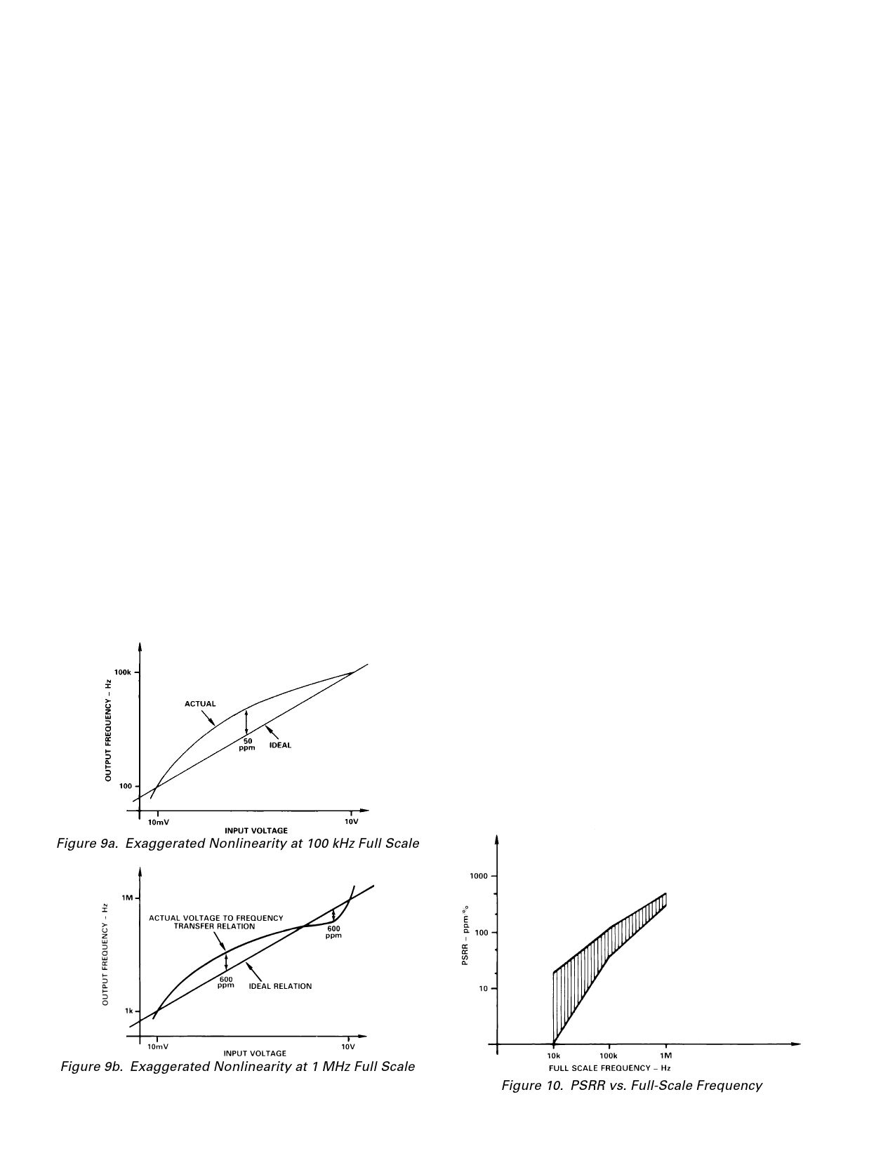
NONLINEARITY SPECIFICATION
The linearity error of the AD650 is specified by the endpoint
method. That is, the error is expressed in terms of the deviation
from the ideal voltage to frequency transfer relation after cali-
brating the converter at full scale and “zero”. The nonlinearity
will vary with the choice of one-shot capacitor and input resistor
(see Figure 3). Verification of the linearity specification requires
the availability of a switchable voltage source (or a DAC) having
a linearity error below 20 ppm, and the use of very long mea-
surement intervals to minimize count uncertainties. Every
AD650 is automatically tested for linearity, and it will not usu-
ally be necessary to perform this verification, which is both te-
dious and time consuming. If it is required to perform a
nonlinearity test either as part of an incoming quality screening
or as a final product evaluation, an automated “bench-top”
tester would prove useful. Such a system based on the Analog
Devices’ LTS-2010 is described in Reference 2.
The voltage-to-frequency transfer relation is shown in Figure 9
with the nonlinearity exaggerated for clarity. The first step in
determining nonlinearity is to connect the endpoints of the
operating range (typically at 10 mV and 10 V) with a straight
line. This straight line is then the ideal relationship which is
desired from the circuit. The second step is to find the differ-
ence between this line and the actual response of the circuit at a
few points between the endpoints—typically ten intermediate
points will suffice. The difference between the actual and the
ideal response is a frequency error measured in hertz. Finally,
these frequency errors are normalized to the full-scale frequency
and expressed either as parts per million of full scale (ppm) or
parts per hundred of full scale (%). For example, on a 100 kHz
full scale, if the maximum frequency error is 5 Hz, the nonlin-
earity would be specified as 50 ppm or 0.005%. Typically on the
100 kHz scale, the nonlinearity is positive and the maximum
value occurs at about midscale (Figure 9a). At higher full-scale
frequencies, (500 kHz to 1 MHz), the nonlinearity becomes “S”
shaped and the maximum value may be either positive or nega-
tive. Typically, on the 1 MHz scale (RIN = 16.9k, COS =
51 pF) the nonlinearity is positive below about 2/3 scale and is
negative above this point. This is shown graphically in Figure 9b.
PSRR
The power supply rejection ratio is a specification of the change
in gain of the AD650 as the power supply voltage is changed.
The PSRR is expressed in units of parts-per-million change of
the gain per percent change of the power supply—ppm/%. For
example, consider a VFC with a 10 volt input applied and an
output frequency of exactly 100 kHz when the power supply
potential is ± 15 volts. Changing the power supply to ± 12.5 volts
is a 5 volt change out of 30 volts, or 16.7%. If the output fre-
quency changes to 99.9 kHz, the gain has changed 0.1% or
1000 ppm. The PSRR is 1000 ppm divided by 16.7% which
equals 60 ppm/%.
The PSRR of the AD650 is a function of the full-scale operating
frequency. At low full-scale frequencies the PSRR is determined
by the stability of the reference circuits in the device and can be
very good. At higher frequencies there are dynamic errors which
become more important than the static reference signals, and
consequently the PSRR is not quite as good. The values of PSRR
are typically 0 ± 20 ppm/% at 10 kHz full-scale frequency (RIN
= 40 k, COS = 3300 pF). At 100 kHz (RIN = 40k, COS = 330 pF)
the PSRR is typically +80 ± 40 ppm/%, and at 1 MHz (RIN =
16.9 kΩ, COS = 51 pF) the PSRR is +350 ± 50 ppm/%. This in-
formation is summarized graphically in Figure 10.
Figure 9a. Exaggerated Nonlinearity at 100 kHz Full Scale
Figure 9b. Exaggerated Nonlinearity at 1 MHz Full Scale
2“V-F Converters Demand Accurate Linearity Testing,” by L. DeVito,
(Electronic Design, March 4, 1982).
–8–
Figure 10. PSRR vs. Full-Scale Frequency
REV. A
Share Link: 