AD650KP Просмотр технического описания (PDF) - Analog Devices
Номер в каталоге
Компоненты Описание
Список матч
AD650KP Datasheet PDF : 12 Pages
| |||
AD650
AUTO ZERO CIRCUIT
In order to exploit the full dynamic range of the AD650 VFC,
very small input voltages will need to be converted. For example,
a six decade dynamic range based on a full scale of 10 volts will
require accurate measurement of signals down to 10 µV. In
these situations a well-controlled input offset voltage is impera-
tive. A constant offset voltage will not affect dynamic range but
simply shift all of the frequency readings by a few hertz. How-
ever, if the offset should change, then it will not be possible to
distinguish between a small change in a small input voltage and
a drift of the offset voltage. Hence, the usable dynamic range is
less. The circuit shown in Figure 13 provides automatic adjust-
ment of the op amp offset voltage. The circuit uses an AD582
sample and hold amplifier to control the offset and the input
voltage to the VFC is switched between ground and the signal to
be measured via an AD7512DI analog switch. The offset of the
AD650 is adjusted by injecting a current into or drawing a cur-
rent out of Pin 13. Note that only one of the offset null pins is
used. During the “VFC Norm” mode, the SHA is in the hold
mode and the hold capacitor is very large, 0.1 µF, to hold the
AD650 offset constant for a long period of time.
in a loop requires a single zero for compensation. Note that the
3.6 kΩ resistor from Pin 1 of the AD650 to the negative supply
is not part of the auto-zero circuit, but rather it is required for
VFC operation at 1 MHz.
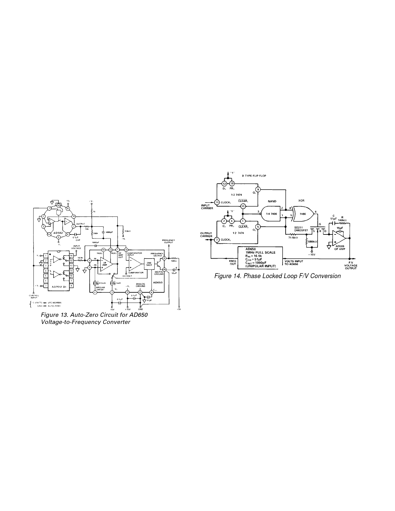
PHASE LOCKED LOOP F/V CONVERSION
Although the F/V conversion technique shown in Figure 6 is
quite accurate and uses only a few extra components, it is very
limited in terms of signal frequency response and carrier feed-
through. If the carrier (or input) frequency changes instanta-
neously, the output cannot change very rapidly due to the
integrator time constant formed by CINT and RIN. While it is
possible to decrease the integrator time constant to provide
faster settling of the F-to-V output voltage, the carrier feed-
through will then be larger. For signal frequency response in
excess of 2 kHz, a phase locked F/V conversion technique such
as the one shown in Figure 14 is recommended.
Figure 13. Auto-Zero Circuit for AD650
Voltage-to-Frequency Converter
When the circuit is in the “Auto Zero” mode the SHA is in
sample mode and behaves like an op amp. The circuit is a varia-
tion of the classical two amplifier servo loop, where the output
of the Device Under Test (DUT)—here the DUT is the AD650
op amp—is forced to ground by the feedback action of the con-
trol amplifier—the SHA. Since the input of the VFC circuit is
connected to ground during the auto zero mode, the input cur-
rent which can flow is determined by the offset voltage of the
AD650 op amp. Since the output of the integrator stage is
forced to ground it is known that the voltage is not changing (it
is equal to ground potential). Hence if the output of the integra-
tor is constant, its input current must be zero, so the offset volt-
age has been forced to be zero. Note that the output of the
DUT could have been forced to any convenient voltage other
than ground. All that is required is that the output voltage be
known to be constant. Note also that the effect of the bias cur-
rent at the inverting input of the AD650 op amp is also nulled in
this circuit. The 1000 pF capacitor shunting the 200 kΩ resistor is
compensation for the two amplifier servo loop. Two integrators
3“Phase lock Techniques,” 2nd Edition, by F.M. Gardner, (John Wiley and
Sons, 1979)
Figure 14. Phase Locked Loop F/V Conversion
In a phase locked loop circuit, the oscillator is driven to a fre-
quency and phase equal to an input reference signal. In applica-
tions such as a synthesizer, the oscillator output frequency is
first processed through a programmable “divide by N” before
being applied to the phase detector as feedback. Here the oscil-
lator frequency is forced to be equal to “N times” the reference
frequency and it is this frequency output which is the desired
output signal and not a voltage. In this case, the AD650 offers
compact size and wide dynamic range.
In signal recovery applications of a PLL, the desired output sig-
nal is the voltage applied to the oscillator. In these situations a
linear relationship between the input frequency and the output
voltage is desired; the AD650 makes a superb oscillator for FM
demodulation. The wide dynamic range and outstanding linear-
ity of the AD650 VFC allow simple embodiment of high perfor-
mance analog signal isolation or telemetry systems. The circuit
shown in Figure 14 uses a digital phase detector which also pro-
vides proper feedback in the event of unequal frequencies. Such
phase-frequency detectors (PFDs) are available in integrated
form. For a full discussion of phase lock loop circuits see
Reference 3.
An analysis of this circuit must begin at the 7474 dual D flip
flop. When the input carrier matches the output carrier in both
phase and frequency, the Q outputs of the flip flops will rise at
exactly the same time. With two zeros, then two ones on the in-
puts of the exclusive or (XOR) gate, the output will remain low
keeping the DMOS FET switched off. Also, the NAND gate
will go low resetting the flip-flops to zero. Throughout the
–10–
REV. A
Share Link: 