AD650KP Просмотр технического описания (PDF) - Analog Devices
Номер в каталоге
Компоненты Описание
Список матч
AD650KP Datasheet PDF : 12 Pages
| |||
entire cycle just described, the DMOS integrator gate remained
off, allowing the voltage at the integrator output to remain un-
changed from the previous cycle. However, if the input carrier
leads the output carrier by a few degrees, the XOR gate will be
turned on for the small time span that the two signals are mis-
matched. Since Q2 will be low during the mismatch time, a
negative current will be fed into the integrator, causing its out-
put voltage to rise. This in turn will increase the frequency of
the AD650 slightly, driving the system towards synchronization.
In a similar manner, if the input carrier lags the output carrier,
the integrator will be forced down slightly to synchronize the
two signals.
Using a mathematical approach, the ± 25 µA pulses from the
phase detector are incorporated into the phase detector gain,
Kd.
Kd
=
25 µA
2π
=
4
× 10–6
amperes /radian
(9)
Also, the V/F converter is configured to produce 1 MHz in
response to a 10 volt input, so its gain Ko, is:
Ko
=
2
π × 1 × 106
10 V
Hz
=
6.3 × 10⁵
radians
volt • sec
(10)
The dynamics of the phase relationship between the input and
output signals can be characterized as a second order system
with natural frequency ωn:
ωn =
KoKd
C
(11)
and damping factor
ζ= R
C KoKd
2
(12)
For the values shown in Figure 14, these relations simplify to a
natural frequency of 35 kHz with a damping factor of 0.8.
For those desiring a simple approach to determining component
values for other PLL frequencies and VFC full-scale voltage, the
following cookbook steps can be used:
AD650
1. Determine Ko (in units of radians per volt second) from the
maximum input carrier frequency FMAX (in hertz) and the
maximum output voltage VMAX.
Ko
=
2
π × FMAX
VMAX
(13)
2. Calculate a value for C based upon the desired loop band-
width, fn. Note that this is the desired frequency range of the
output signal. The loop bandwidth (fn) is not the maximum
carrier frequency (fMAX): the signal may be very narrow even
though it is transmitted over a 1 MHz carrier.
C
=
Ko
f n2
•
1
×
10–7
V
Rad
•F
• sec
C units FARADS
fn units HERTZ (14)
Ko units RAD/VOLT•SEC
3. Calculate R to yield a damping factor of approximately 0.8
using this equation:
R
=
fn
Ko
• 2.5 × 10⁶
Rad • Ω
V
R units OHMS
fn units HERTZ (15)
Ko units RAD/VOLT•SEC
If in actual operation the PLL overshoots or hunts excessively
before reaching a final value, the damping factor may be raised
by increasing the value of R. Conversely, if the PLL is
overdamped, a smaller value of R should be used.
PLL PERFORMANCE
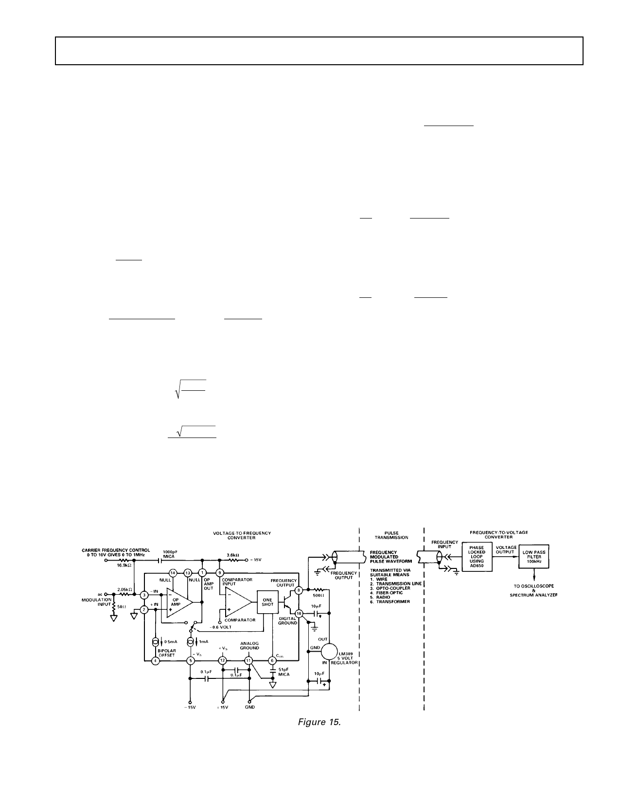
The performance of the PLL circuit is demonstrated by the
system shown in Figure 15; an analog signal is converted into a
frequency, and then this frequency is converted back into an
analog voltage by the PLL.
The source of the frequency input signal used to drive the PLL
is an AD650 with two separate inputs: one for dc to set the car-
rier frequency, and one for ac to establish a modulation. Note
how the summing junction input to the AD650 allows such flex-
ibility. The output frequency is then relayed to the PLL via a
REV. A
Figure 15.
–11–
Share Link: 