ZR36015 Просмотр технического описания (PDF) - Unspecified
Номер в каталоге
Компоненты Описание
Список матч
ZR36015 Datasheet PDF : 27 Pages
| |||
PRELIMINARY
ZR36015
with the ZR36050, the COE signal is connected to the ZR36050’s “COMP” output.
The DSYNC signal synchronized 64 byte block transfers between the ZR36015 and the ZR36050.
The STOP signal indicates to the sending device that the receiving device is not ready for more data. New blocks of data will not be
sent to the receiving device until the STOP signal becomes inactive.
The EOS signal indicates the end of each component of a scan. This active low signal is an output in encoding modes. EOS indicates
the last image data sample of the last block of each scan leaving the ZR36015. In encoding modes, EOS is output regardless of the
STOP signal.
EOS is an input signal in the decoding mode. It is input together with the last image data sample of the last block of each scan entering
the ZR36015.
The width of EOS is one SYSCLK cycle in encoding mode, and must be on SYSCLK cycle in decoding mode.
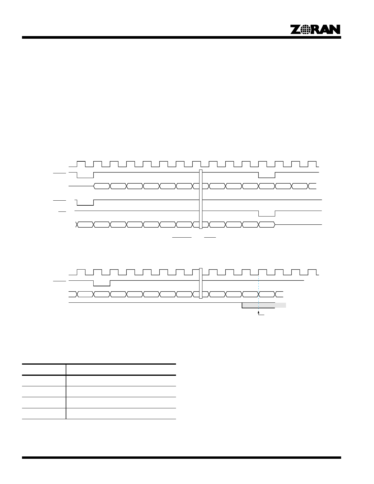
Figure 22 shows the functional timing for the DSYNC and EOS signals relative to the BDATA(7:0) data and SYSCLK.
The functional timing relationship for the STOP (when used as an input during compression mode) is given in Figure 23.
SYSCLK
DSYNC
BDATA (7:0)
1
2
3
4
5
6
61
62
63
64
1
2
3
DSYNC
EOS
BDATA (7:0)
64
1
2
3
4
5
6
61
62
63
64
Figure 25. Functional Timing for DSYNC and EOS Relative to BDATA(7:0)
SYSCLK
DSYNC
BDATA (7:0)
STOP
62
63
0
1
2
3
4
59
60
61
62
63
If STOP is low, do not output DSYNC
If STOP is High, output DSYNC
Figure 26. Functional Timing for STOP When Used as an Input
The “delay to memory write” indicates the number of clock cycles it takes for the pixel data to propagate through the ZR36015 to the
strip buffer memory. This value is shown in the table below.
Table 6: Delay to Memory Write
Mode
Delay (in number of SYSCLKS)
0
2 or 3
1
10 or 11
2
10 or 11
3
10 or 11
In the table above, the smaller value corresponds to the even clock PXDATA element, and the larger value corresponds to the odd
PXDATA element (the ZR36015 writes 16 bits to the strip memroy at a time).
20
Share Link: 