ZR36015 Просмотр технического описания (PDF) - Unspecified
Номер в каталоге
Компоненты Описание
Список матч
ZR36015 Datasheet PDF : 27 Pages
| |||
PRELIMINARY
ZR36015
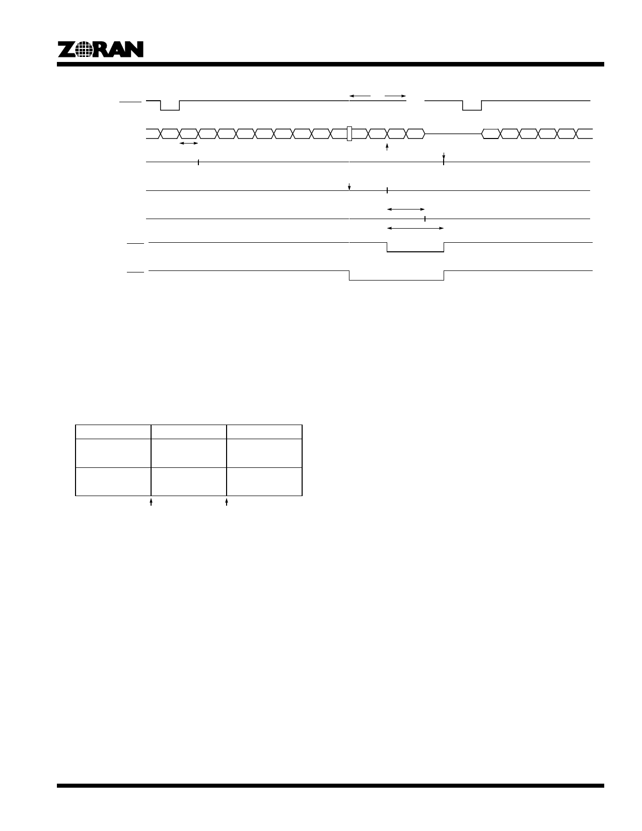
N1
DSYNC
BDATA (7:0)
Write to Strip Buffer
64 1 2 3 4
Delay of internal
processing
Final line data of the readout side buffer
Read From Strip Buffer
5678
1 block data
Check if all contents of the pixel
side buffer have been read out.
62 63 64
Buffer selection point
Check if all contents of the coder
side buffer have been entered.
123456
PXDATA
PAX
Delay of internal
processing
The coder side buffer is
monitored as required
CBSY
STOP
Figure 18. Example of Double-Sided Buffer Selection Timing - In Decoding
Strip Buffer Memory Format
Two SRAMs form a strip buffer. The 16-bit wide strip buffer is divided into 2 areas at point α * HWidth. Where:
α = K * L * HWidth * D
Memory A
(lower 8 bits)
Memory B
(Upper 8 bits)
Low Memory
Write Area
(RD Area)
Write Area
(RD Area)
High Memory
Read Area
(Write Area)
Read Area
(Write Area)
Address 0
Address = α * HWidth
An example of the amount of data stored in the strip buffer for each component of an active region of 704 x 240 is given in Figure 16.
15
Share Link: 