ZR36015 Просмотр технического описания (PDF) - Unspecified
Номер в каталоге
Компоненты Описание
Список матч
ZR36015 Datasheet PDF : 27 Pages
| |||
PRELIMINARY
ZR36015
Component interleave
sequence for blocks of data
(as seen on the code data bus)
MODE1:0 = 00 Y0 Y1 Y2 Y3 Y4 Y5
MODE1:0 = 01 Y00 Y01 U00 V00 Y02 Y03 U01 V01
MODE1:0 = 10 Y00 Y01 Y10 Y11 01U0 01V0 Y02 Y03 Y12 Y13 01U1 01V1
MODE1:0 = 11 Y00 Y01 Y02 Y03 U00 V00 Y04 Y05 Y06 Y07 U01 V01
8
8
8
8
MODE = 01 8 Y00 Y01
U00
V00
8
8
8
MODE = 10
Y00
Y01
8 Y10 Y11
8
8
8
8
01U0
01V0
8
8
8
8
8
8
8
8
MODE = 11 8 Y00 Y01 Y02 Y03
U00
V00
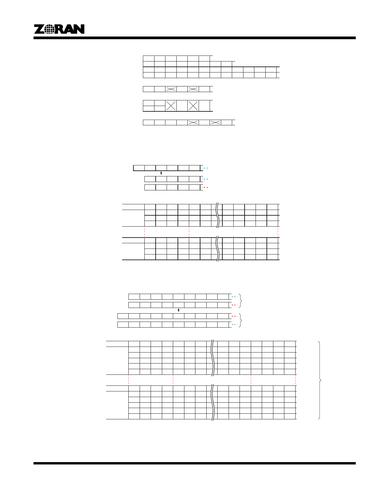
Note: YX notation indicates the “x”th block of data for component Y
Figure 20. Memory Format - Write Area
Pixel Data 0Y0 0Y1 0Y2 0Y3 0Y4 0Y5
Memory Data <15:8>
Memory Data <7:0>
0Y0 0Y2 0Y4 0Y6 0Y8
0Y1 0Y3 0Y5 0Y7 0Y9
Strip Memory
A Memory
B Memory
MADD
0
$20
$40
MADD
0
$20
$40
0
0Y0
0Y8
0Y16
1
0Y2
0Y10
0Y18
2
0Y4
0Y12
0Y20
3
0Y6
0Y14
0Y22
4
1Y0
1Y8
1Y16
5
1Y2
1Y10
1Y18
1st Line
Data
2nd Line
Data
0
0Y1
0Y9
0Y17
1
0Y3
0Y11
0Y19
2
0Y5
0Y13
0Y21
3
0Y7
0Y15
0Y23
4
1Y1
1Y9
1Y17
5
1Y3
1Y11
1Y19
1B
6Y6
6Y14
6Y22
1C
7Y0
7Y8
7Y16
1D
7Y2
7Y10
7Y18
1E
7Y4
7Y12
7Y20
1F
7Y6
7Y14
7Y22
1st Block
2nd Block
3rd Block
6th Line
Data
7th Line
Data
1B
6Y7
6Y15
6Y23
1C
7Y1
7Y9
7Y17
1D
7Y3
7Y11
7Y19
1E
7Y5
7Y13
7Y21
1F
7Y7
7Y15
7Y23
1st Block
2nd Block
3rd Block
Note: aYb notation indicates the Y component of the pixel element in row “a” and column “b”.
Figure 21. Memory Format - MODE 1:0 = 00
Pixel Data <15:8>
Pixel Data <7:0>
0Y0 0Y1 0Y2 0Y3 0Y4 0Y5 0Y6 0Y7 0Y8
0U0 0V0 0U1 0V1 0U2 0V2 0U3 0V3 0U4
Data Sequence on Pixel Bus
Memory Data <15:8> 0Y0 0Y2 0Y4 0Y6 0U0 0U2 0V0 0V2 0Y8 0Y10
Memory Data <7:0> 0Y1 0Y3 0Y5 0Y7 0U1 0U3 0V1 0V3 0Y9 0Y11
Data Sequence on Memory Data Bus
Strip Memory
A Memory
A Memory
MADD
0
$20
$40
$60
$80
MADD
0
$20
$40
$60
$80
0
0Y0
0Y8
0U0
0V0
0Y16
1
0Y2
0Y10
0U2
0V2
0Y18
2
0Y4
0Y12
0U4
0V4
0Y20
3
0Y6
0Y14
0U6
0V6
0Y22
4
1Y0
1Y8
1U0
1V0
1Y16
5
1Y2
1Y10
1U2
1V2
1Y18
6
1Y4
1Y12
1U4
1V4
1Y20
1st Line
Data
2nd Line
Data
0
0Y1
0Y9
0U1
0V1
0Y17
1
0Y3
0Y11
0U3
0V3
0Y19
2
0Y5
0Y13
0U5
0V5
0Y21
3
0Y7
0Y15
0U7
0V7
0Y23
4
1Y1
1Y9
1U1
1V1
1Y17
5
1Y3
1Y11
1U3
1V3
1Y19
6
1Y5
1Y13
1U5
1V5
1Y21
19
6Y2
6Y10
6U2
6V2
6Y18
1A
6Y4
6Y12
6U4
6V4
6Y20
1B
6Y6
6Y14
6U6
6V6
6Y22
1C
7Y0
7Y8
7U0
7V0
7Y16
1D
7Y2
7Y10
7U2
7V2
7Y18
1E
7Y4
7Y12
7U4
7V4
7Y20
1F
7Y6
7Y14
7U6
7V6
7Y22
1st Block
2nd Block
3rd Block
4th Block
5th Block
7th Line
Data
8th Line
Data
19
6Y3
6Y11
6U3
6V3
6Y19
1A
6Y5
6Y13
6U5
6V5
6Y21
1B
6Y7
6Y15
6U7
6V7
6Y23
1C
7Y1
7Y9
7U1
7V1
7Y17
1D
7Y3
7Y11
7U3
7V3
7Y19
1E
7Y5
7Y13
7U5
7V5
7Y21
1F
7Y7
7Y15
7U7
7V7
7Y23
1st Block
2nd Block
3rd Block
4th Block
5th Block
Note: aYb notation indicates the Y component of the pixel element in row “a” and column “b”.
Figure 22. Memory Format - MODE 1:0 = 01
Data Storage in
Strip Memory
17
Share Link: 