LH52D1000 Просмотр технического описания (PDF) - Sharp Electronics
Номер в каталоге
Компоненты Описание
Список матч
LH52D1000 Datasheet PDF : 12 Pages
| |||
LH52D1000
CMOS 1M (128K × 8) Static RAM
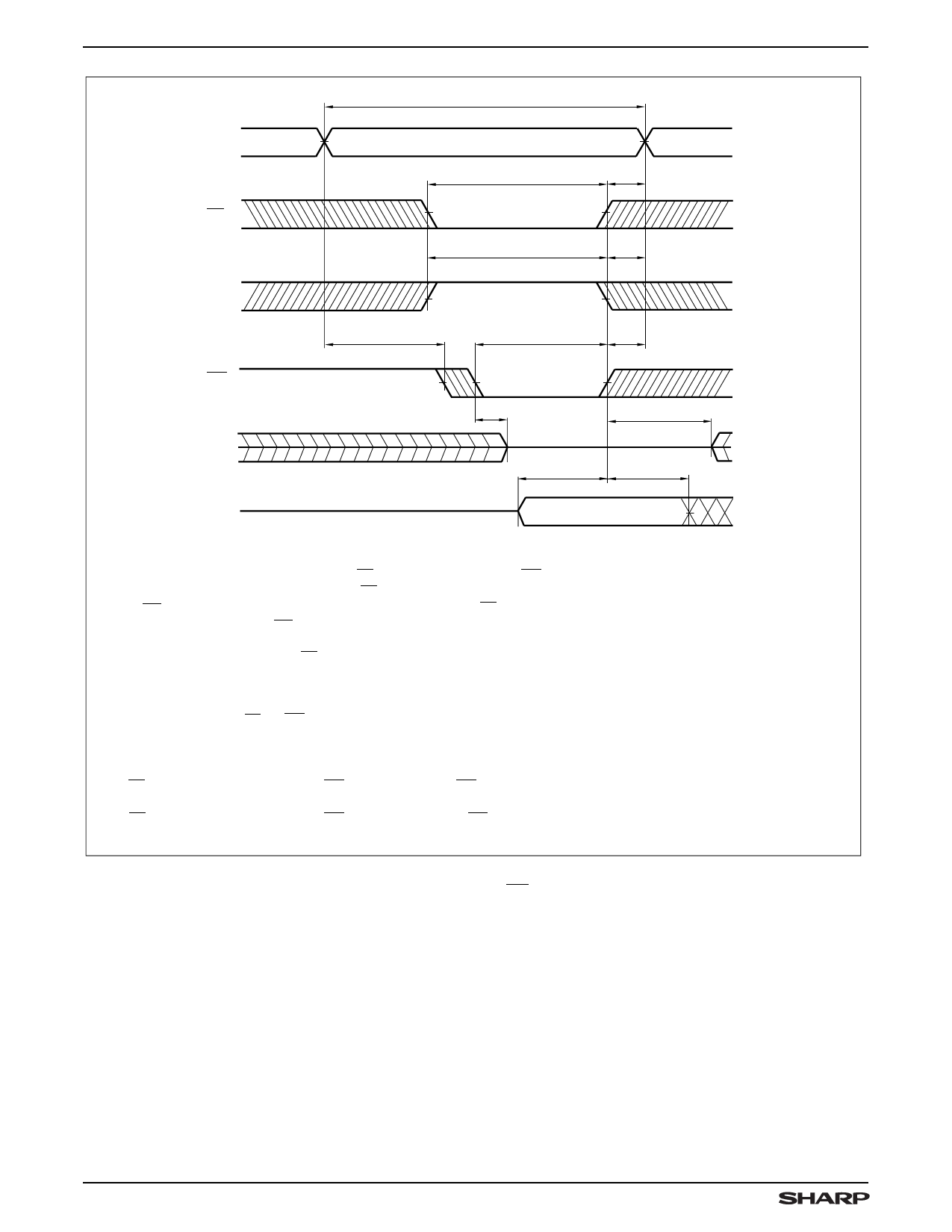
ADDRESS
CE1
CE2
WE
DOUT
DIN
tWC
tCW
(NOTE 2)
tCW
(NOTE 2)
tWR (NOTE 4)
tWR
tAS
(NOTE 3)
(NOTE 6)
tWP
tWR
(NOTE 1)
tWZ
(NOTE 5)
tOW
(NOTE 7)
tDW
tDH
DATA VALID
NOTES:
1. A write occurs during the overlap of a LOW CE1, a HIGH CE2 and a LOW WE,
A write begins at the latest transition among CE1 going LOW, CE2 going HIGH
and WE going LOW. A write ends at the earliest transition among CE1 going
HIGH. CE2 going LOW and WE going HIGH. tWP is measured from the beginning
of write to the end of write.
2. tCW is measured from the later of CE1 going LOW or CE2 going HIGH to the
end of write.
3. tAS is measured from the address valid to the beginning of write.
4. tWR is measured from the end of write to the address change. tWR1 applies
in case a write ends at CE1 or WE going HIGH. tWR2 applies in case a write
ends at CE2 going LOW.
5. During this period, I/O pins are in the output state, therefore the input signals
of opposite phase to the outputs must not be applied.
6. If CE1 goes LOW simultaneously with WE going LOW or after WE going LOW,
the outputs remain in high impedance state.
7. If CE1 goes HIGH simulaneously with WE going HIGH or before WE going HIGH,
the outputs remain in high impedance state.
Figure 5. Write Cycle (OE Low Fixed)
52D1000S-5
8
Share Link: 