MT8960 Просмотр технического описания (PDF) - Zarlink Semiconductor Inc
Номер в каталоге
Компоненты Описание
Список матч
MT8960 Datasheet PDF : 32 Pages
| |||
MT8960/61/62/63/64/65/66/67
[( )( )] V X
Ref
2C 16.5 + S
128
32
±VOFFSETC≠0
where C = chord number (0-7)
S = step number (0-15)
VRef is a high impedance input with a varying capacitive load of up to 40 pF.
Data Sheet
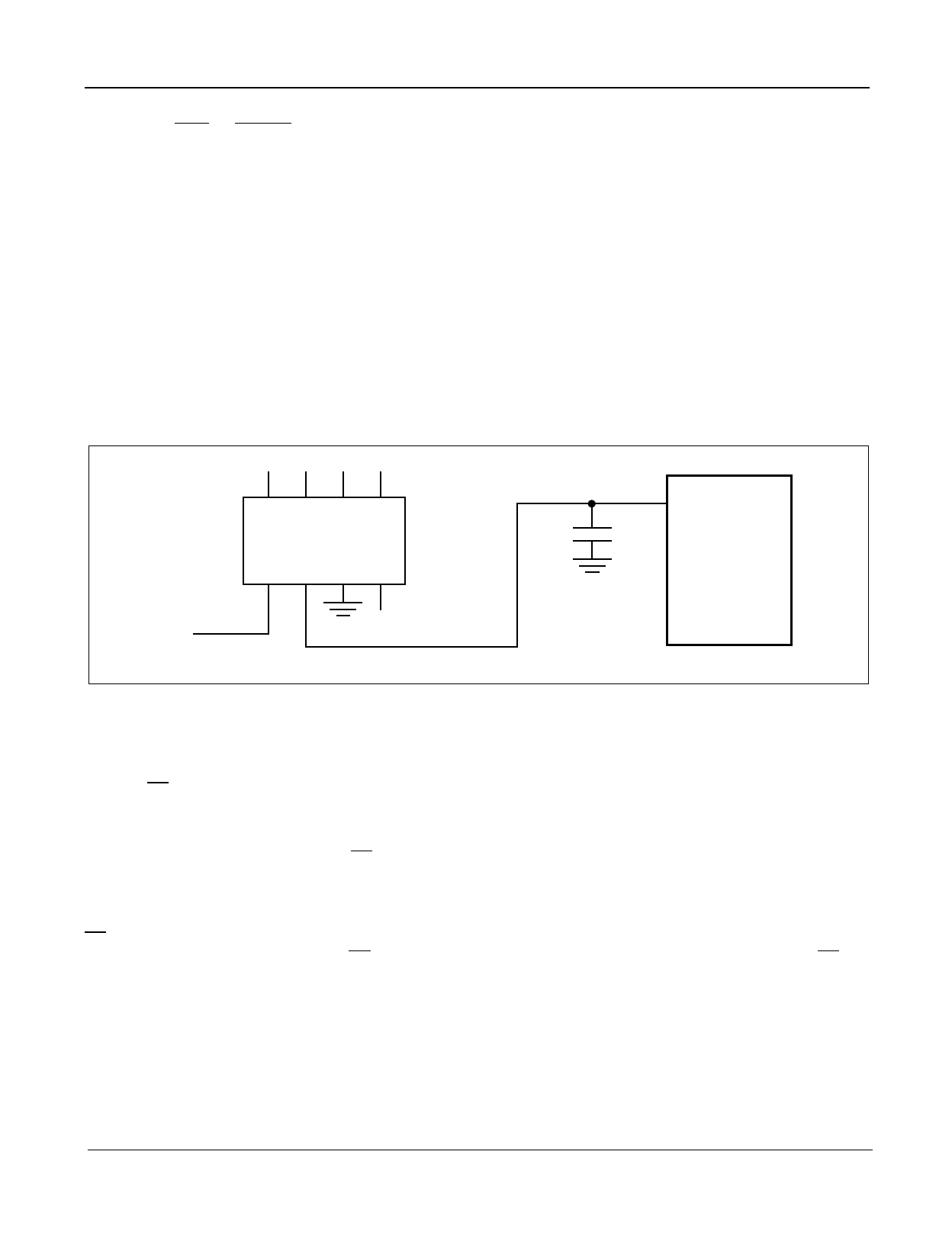
The recommended reference voltage for the MT8960 series of codecs is 2.5 V ±0.5%. The output voltage from the
reference source should have a maximum temperature coefficient of 100 ppm/C°. This voltage should have a total
regulation tolerance of ±0.5% both for changes in the input voltage and output loading of the voltage reference
source. A voltage reference circuit capable of meeting these specifications is shown in Figure 5. Analog
Devices’AD1403A voltage reference circuit is capable of driving a large number of codecs due to the high input
impedance of the VRef input. Normal precautions should be taken in PCB layout design to minimize noise coupling
to this pin. A 0.1 µF capacitor connected from VRef to ground and located as close as possible to the codec is
recommended to minimize noise entering through VRef. This capacitor should have good high frequency
characteristics.
NC NC NC NC
8765
AD1403A
1234
0.1 µF
VRef
MT8960-67
FILTER/CODEC
NC
+5 V
2.5 V
Figure 5 - Typical Voltage Reference Circuit
Timing
The codec operates in a synchronous manner (see Figure 9a). The codec is activated on the first positive edge of
C2i after F1i has gone low. The digital output at DSTo (which is a three-state output driver) will then change from
a high impedance state to the sign bit of the encoded PCM word to be output. This will remain valid until the next
positive edge, when the next most significant bit will be output.
On the first negative clock edge (after F1i signal has been internally synchronized and CA is at GNDD or VEE) the
logic signal present at DSTi will be clocked into the input shift register as the sign bit of the incoming PCM word.
The eight-bit word is thus input at DSTi on negative edges of C2i and output at DSTo on positive edges of C2i.
F1i must return to a high level after the eighth clock pulse causing DSTo to enter high impedance and
preventing further input data to DSTi. F1i will continue to be sampled on every positive edge of C2i. (Note: F1i may
subsequently be taken low during the same sampling frame to enable entry of serial data into CSTi. This occurs
usually mid-frame, in conjunction with CA=VDD, in order to enter an 8-bit control word into Register B. In this case,
PCM input and output are inhibited by CA at VDD.)
Internally the codec will then perform a decode cycle on the newly input PCM word. The sampled and held analog
signal thus decoded will be updated 25 µs from the start of the cycle. After this the analog input from the filter is
sampled for 18 µs, after which digital conversion takes place during the remaining 82 µs of the sampling cycle.
6
Zarlink Semiconductor Inc.
Share Link: 