MT8960 Просмотр технического описания (PDF) - Zarlink Semiconductor Inc
Номер в каталоге
Компоненты Описание
Список матч
MT8960 Datasheet PDF : 32 Pages
| |||
MT8960/61/62/63/64/65/66/67
Data Sheet
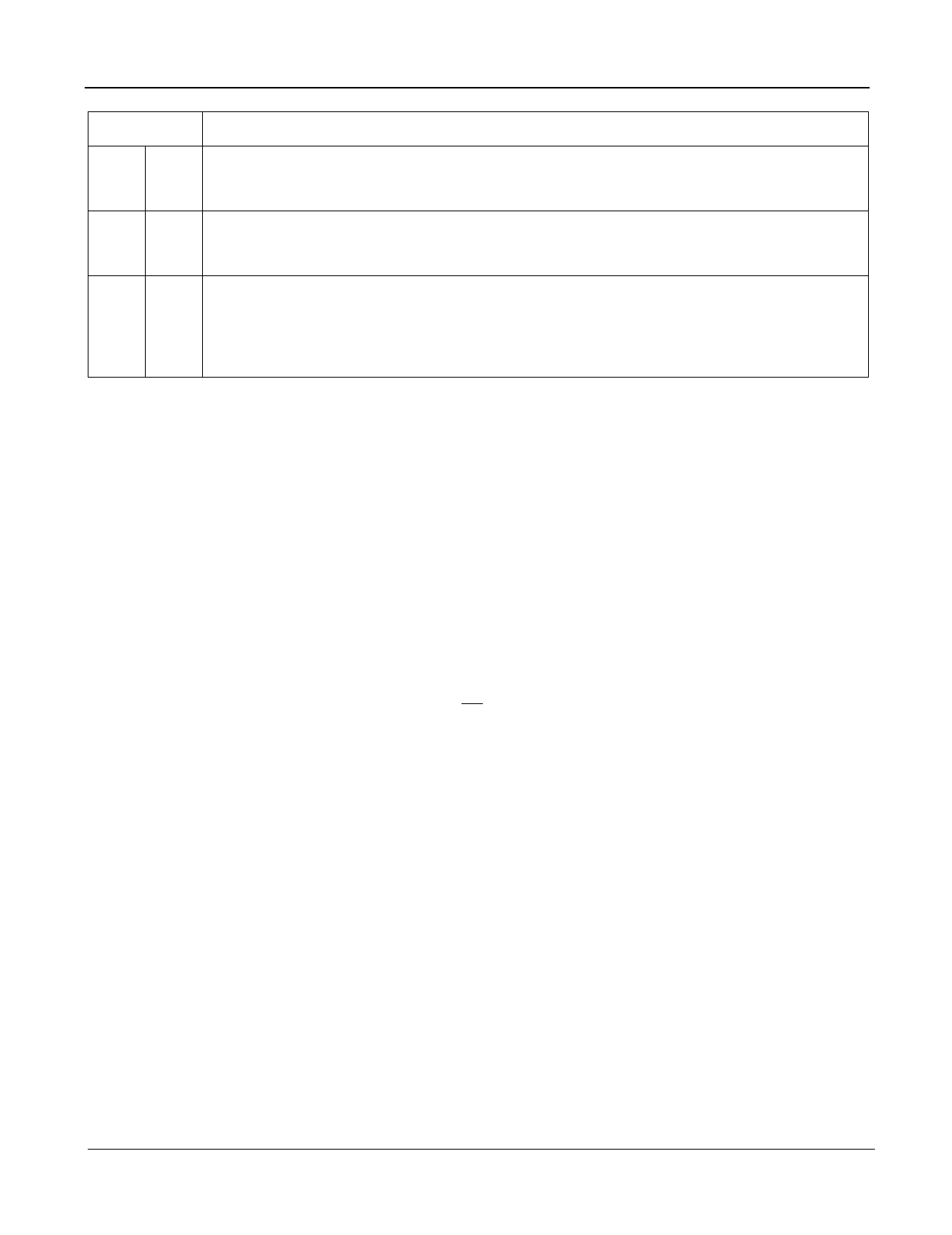
BITS 0-2
0
1
1
0
1
1
LOGIC CONTROL OUTPUTS SD0-SD2
Transmit filter testing, i.e.:
Transmit filter input connected to VX input
Receive filter and Buffer disconnected from VR
Receive filter testing, i.e.:
Receive filter input connected to VX input
Receive filter input disconnected from codec
Codec testing i.e.:
Codec analog input connected to VX
Codec analog input disconnected from transmit filter output
Codec analog output connected to VR
VR disconnected from receive filter output
Table 3 - Control States - Register B
Powerdown
Powerdown of the chip is achieved in several ways:
Internal Control:
1) Initial Power-up. Initial application of VDD and VEE causes powerdown for a period of 25 clock cycles and
during this period the chip will accept input only from C2i. The B-register is reset to zero forcing SD0-5 to
be inactive. Bits 0-5 of Register A (gain adjust bits) are forced to zero and bits 6 and 7 of Register A
become logic high thus reinforcing the powerdown.
2) Loss of C2i. Powerdown is entered 10 to 40 µs after C2i has assumed a continuous logic high (VDD). In
this condition the chip will be in the same state as in (1) above.
Note: If C2i stops at a continuous logic low (GNDD), the digital data and status is indeterminate.
External Control:
1) Register A. Powerdown is controlled by bits 6 and 7 (when both at logic high) of Register A which in turn
receives its control word input via CSTi, when F1i is low and CA input is either at VEE or GNDD. Power is
removed from the filters and analog sections of the chip. The analog output buffer at VR will be connected
to GNDA. DSTo becomes high impedance and the clocks to the majority of the logic are stopped. SD
outputs are unaffected and may be updated as normal.
2) CSTi Input. With CA at VEE and CSTi held at continuous logic high the chip assumes the same state as
described in External Control (1) above.
11
Zarlink Semiconductor Inc.
Share Link: 