MT8960 Просмотр технического описания (PDF) - Zarlink Semiconductor Inc
Номер в каталоге
Компоненты Описание
Список матч
MT8960 Datasheet PDF : 32 Pages
| |||
MT8960/61/62/63/64/65/66/67
Data Sheet
MT8960/61/64/65
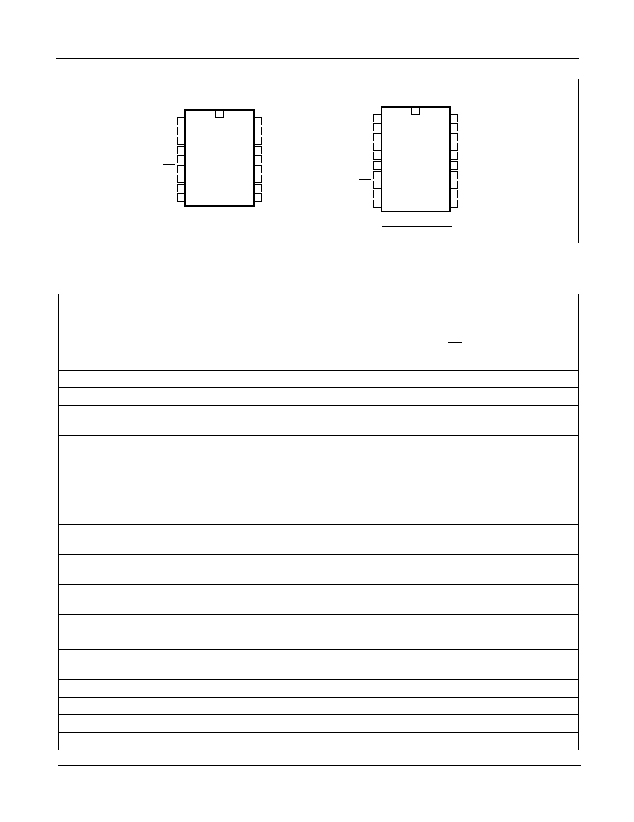
CSTi 1
DSTi 2
C2i 3
DSTo 4
VDD 5
F1i 6
CA 7
SD3 8
SD2 9
18 GNDD
17 VRef
16 GNDA
15 VR
14 ANUL
13 VX
12 VEE
11 SD0
10 SD1
18 PIN PDIP
MT8962/63/66/67
CSTi 1
DSTi 2
C2i 3
DSTo 4
VDD 5
SD5 6
SD4 7
F1i 8
CA 9
SD3 10
20 GNDD
19 VRef
18 GNDA
17 VR
16 ANUL
15 VX
14 VEE
13 SD0
12 SD1
11 SD2
20 PIN PDIP/SOIC
Figure 2 - Pin Connections
Pin Description
Pin Name
Description
CSTi
DSTi
Control ST-BUS In is a TTL-compatible digital input used to control the function of the filter/codec.
Three modes of operation may be effected by applying to this input a logic high (VDD), logic low
(GNDD), or an 8-bit serial word, depending on the logic states of CA and F1i.
Functions controlled are: powerdown, filter gain adjust, loopback, chip testing, SD outputs.
Data ST-BUS In accepts the incoming 8-bit PCM word. Input is TTL-compatible.
C2i
DSTo
Clock Input is a TTL-compatible 2.048 MHz clock.
Data ST-BUS Out is a three-state digital output driving the PCM bus with the outgoing 8-bit PCM
word.
VDD Positive power Supply (+5 V).
F1i Synchronization Input is an active low digital input enabling (in conjunction with CA) the PCM input,
PCM output and digital control input. It is internally sampled on every positive edge of the clock, C2i,
and provides frame and channel synchronization.
CA Control Address is a three-level digital input which enables PCM input and output and determines
into which control register (A or B) the serial data, presented to CSTi, is stored.
SD3
SD4-5
System Drive Output is an open drain output of an N-channel transistor which has its source tied to
GNDA. Inactive state is open circuit.
System Drive Outputs are open drain outputs of N-channel transistors which have their source tied
to GNDD. Inactive state is open circuit.
SD0-2 System Drive Outputs are “Totempole“ CMOS outputs switching between GNDD and VDD. Inactive
state is logic low.
VEE
VX
ANUL
VR
GNDA
VRef
GNDD
Negative power supply (-5 V).
Voice Transmit is the analog input to the transmit filter.
Auto Null is used to integrate an internal auto-null signal. A 0.1 µF capacitor must be connected
between this pin and GNDA.
Voice Receive is the analog output of the receive filter.
Analog ground (0 V).
Voltage Reference input to D to A converter.
Digital ground (0 V).
2
Zarlink Semiconductor Inc.
Share Link: 