MT8960 Просмотр технического описания (PDF) - Zarlink Semiconductor Inc
Номер в каталоге
Компоненты Описание
Список матч
MT8960 Datasheet PDF : 32 Pages
| |||
MT8960/61/62/63/64/65/66/67
Data Sheet
MT8961/63
Digital Output
MT8965/67
Digital Output
11111111
11110000
11100000
11010000
11000000
10110000
10100000
10010000
10000000
00000000
00010000
00100000
00110000
01000000
01010000
01100000
01110000
01111111
-2.5V
Bit 7... 0
MSB LSB
10101010
10100101
10110101
10000101
10010101
11100101
11110101
11000101
11010101
01010101
01000101
01110101
01100101
00010101
00000101
00110101
00100101
00101010
-1.25V 0V +1.25V +2.5V
Analog Input Voltage (VIN)
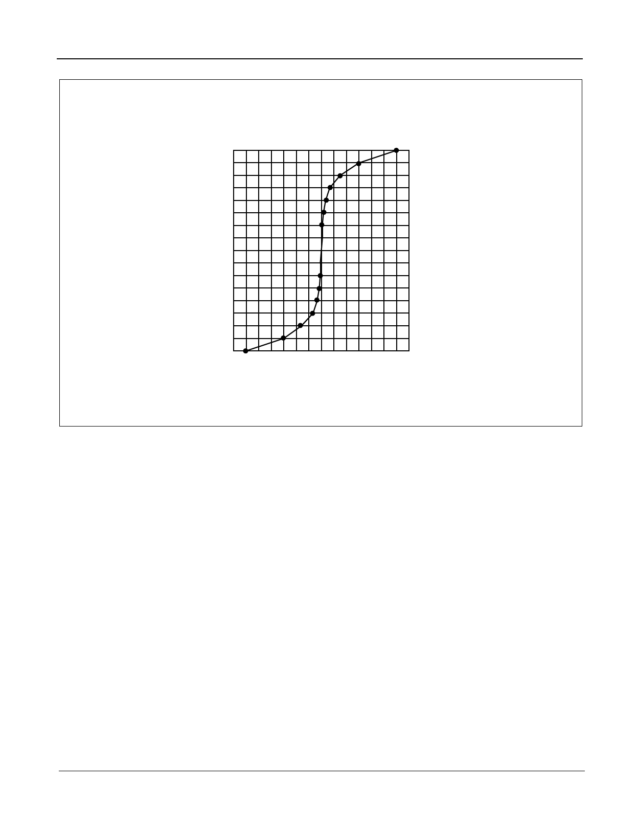
Figure 4 - A-Law Encoder Transfer Characteristic
Functional Description
Figure 1 shows the functional block diagram of the MT8960-67. These devices provide the conversion interface
between the voiceband analog signals of a telephone subscriber loop and the digital signals required in a digital
PCM (pulse code modulation) switching system. Analog (voiceband) signals in the transmit path enter the chip at
VX, are sampled at 8 kHz, and the samples quantized and assigned 8-bit digital values defined by logarithmic PCM
encoding laws. Analog signals in the receive path leave the chip at VR after reconstruction from digital 8-bit words.
Separate switched capacitor filter sections are used for bandlimiting prior to digital encoding in the transmit path
and after digital decoding in the receive path. All filter clocks are derived from the 2.048 MHz master clock input,
C2i. Chip size is minimized by the use of common circuitry performing the A to D and D to A conversion. A
successive approximation technique is used with capacitor arrays to define the 16 steps and 8 chords in the signal
conversion process. Eight-bit PCM encoded digital data enters and leaves the chip serially on DSTi and DSTo
pins, respectively.
Transmit Path
Analog signals at the input (Vx) are firstly bandlimited to 508 kHz by an RC lowpass filter section. This performs the
necessary anti-aliasing for the following first-order sampled data lowpass pre-filter which is clocked at 512 kHz.
This further bandlimits the signal to 124 kHz before a fifth-order elliptic lowpass filter, clocked at 128 kHz, provides
the 3.4 kHz bandwidth required by the encoder section. A 50/60 Hz third-order highpass notch filter clocked at
8 kHz completes the transmit filter path. Accumulated DC offset is cancelled in this last section by a switched-
capacitor auto-zero loop which integrates the sign bit of the encoded PCM word, fed back from the codec and
4
Zarlink Semiconductor Inc.
Share Link: 