AT76C101 Просмотр технического описания (PDF) - Atmel Corporation
Номер в каталоге
Компоненты Описание
Список матч
AT76C101 Datasheet PDF : 13 Pages
| |||
AT76C101
Compressed Data Memory Management
The AT76C101 starts reading/writing data from/to the com-
pressed data memory starting from the address location
specified by the Mem_Start_Addr register. Once a frame
has been processed, the AT76C101 writes the address of
the last compressed data into the Mem_End_Addr register.
The microcontroller uses this information to keep track of
the memory locations having valid images, and to specify
the starting memory address of the next image
Initialization Sequence
The active high RESET signal resets all the AT76C101
resources including the register file. Once the AT76C101
has been reset, the microcontroller can program the chip to
the desired mode of operation. The microcontroller will also
have to load the internal Huffman and Quantization Tables.
Once the internal registers and tables have been initialized,
the microcontroller can initiate a compression/decompres-
sion operation by asserting the Start_Reg register. The
AT76C101 de-asserts this signal after the final image block
is processed. When the AT76C101 completes the process-
ing of an image, it asserts the FRAMEND signal, writes the
address of the last compressed data into the
Mem_End_Addr register and waits for a new Start_Reg
request.
During decompression, the microcontroller has to do some
additional processing of the JPEG data stream. The micro-
controller extracts and process the JPEG header informa-
tion from the compressed data stream. Based on this
header information, the microcontroller then initializes the
internal registers of the AT76C101 and writes the address
of the memory location containing the first compressed
image data (not the start of the JPEG header) into the
Mem_Start_Addr register. It then follows the above men-
tioned initialization sequence.
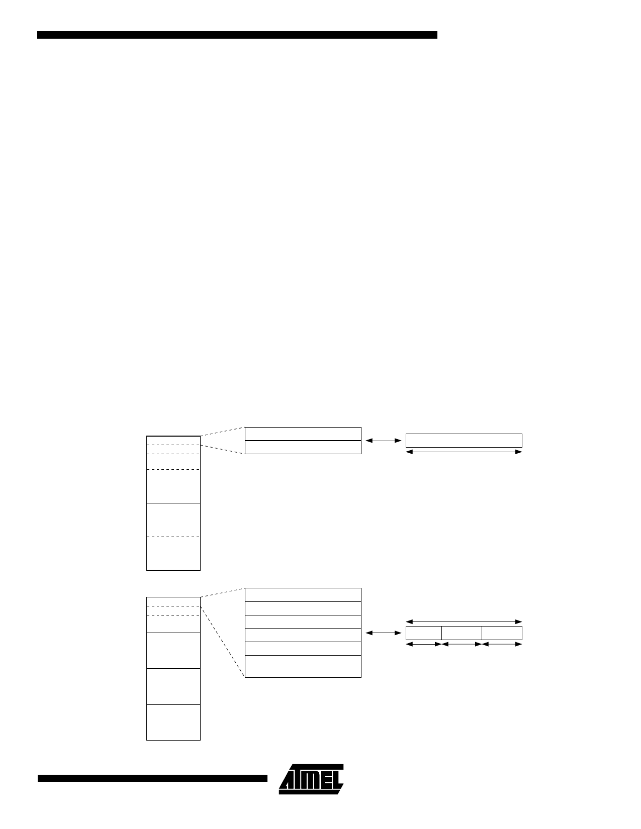
Quantization Table Loading
The on-chip quantization tables must be loaded with the
required values before the normal operation of the chip.
The AT76C101’s quantization table is a 256x16 RAM, and
can store up to four 64-word quantization tables. The upper
half of the RAM area is used to store the compression
quantization tables and the lower half to store the decom-
pression tables. The organization of the quantization RAM
is shown in Figure 4. The Quantization Tables can be
loaded only after the Quant_Table_Load_Enable register
has been set. Once loaded, the quantization tables remain
valid until the power is switched off or until they are repro-
grammed (they are unaffected by RESET). The
Quant_Table_Load_Enable register has to be reset after
the tables are loaded and before normal operation of the
chip can begin.
Figure 4. Internal Memory Organization (Quantization and MaxMin Tables)
0000h
0002h
0000h
0001h
QUANTIZATION VALUE (BITS 7-0)
QUANTIZATION VALUE (BITS 15-8)
0080h
Y
ENCODING
UV
QUANTIZATION VALUE
16 BITS
0100h
0180h
Y
DECODING
UV
QUANTIZATION TABLE
3000h
3008h
3080h
3100h
3180h
DC-Y
DC-UV
AC-Y
AC-UV
3000h
3001h
3002h
3003h
3004h
3005h
3006h
3007h
MAXMIN TABLE
MIN_CODE (BITS 7-0)
MIN_CODE (BITS 15-8)
MAX_CODE (BITS 7-0)
MAX_CODE (BITS 15-8)
VAL_PTR
NOT USED
40 BITS
VAL_PTR MAX_CODE MIN_CODE
8 BITS
16 BITS
16 BITS
5
Share Link: 