AT76C101 Просмотр технического описания (PDF) - Atmel Corporation
Номер в каталоге
Компоненты Описание
Список матч
AT76C101 Datasheet PDF : 13 Pages
| |||
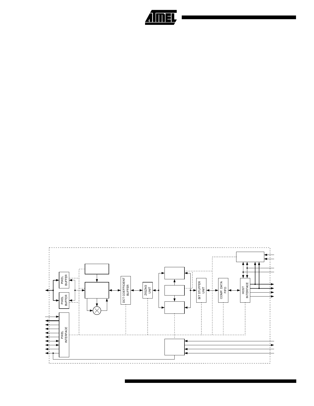
Host Interface
This is a 8-bit interface that allows the AT76C101 to trans-
fer the compressed data to an external memory device.
This interfaces also allows an external microcontrol-
ler/microprocessor (complexity of AT89C51) to access the
internal memory (registers and tables) of the AT76C101.
Two types of transfers can be carried out through this inter-
face: the compressed data transfers and the microcontrol-
ler data accesses.
Compressed Data Mode
The host interface can work with a number of external
memory devices. It has two programmable registers
through which the user can specify up to eight wait states
that allows the chip to interface with slow memory devices.
Data transfers are 8 bit wide and are carried out through
the Data Bus, Address Bus and the control signals
MEM_CS, MASTER_OE and MASTER_WR. The
AT76C101 is the bus master and controls all transfers to
the external memory. Other devices cannot access the
memory while the AT76C101 is in the operating mode.
The cycle time of the compressed data transfer varies from
one to eight CLK cycles. This cycle time is controlled by
two registers, the Read_Cnt_Reg which controls the read
cycle time, and Write_Cnt_Reg which controls the write
cycle time. These registers are programmed by the micro-
controller during initialization. The address bus is also ini-
tialized from the Mem_Start_Addr register, which holds the
start address of the compressed data memory.
Microcontroller Access Mode
In this mode, the main function of the host interface is to
allow external devices, (i.e. microcontroller or a host pro-
cessor) to access the internal memory of the JPEG chip.
Figure 3. Data Control
This is required to program the AT76C101 in the desired
mode of operation, to load the internal quantization and
Huffman tables during initialization, and to read the status
of the chip for testing purposes.
All transfers to the internal memory and tables of the JPEG
codec are 8-bit wide. Data is transferred using the Data
Bus, Address Bus, and the control signals MASTER_WR,
MASTER_OE, MASTER_CS and BUS_BUSY. All transfers
carried out in this mode are controlled by the microcontrol-
ler.
When the AT76C101 chip is operating in normal mode (i.e.
either compression or decompression), it acts as a bus
master on the external memory/microcontroller bus. Since
the AT76C101 has higher priority over the microcontroller
for these bus accesses, the microcontroller has to check
the availability of the bus (by checking BUS_BUSY) before
it can access it. Once all the internal registers of the
AT76C101 are set up and the tables are loaded, the
AT76C101 is activated by setting the Start_Reg register.
Once the compression/decompression operation starts, the
AT76C101 takes control of the bus, and gives it up only
after the chip has processed the image.The microcontroller
can access the internal memory of the AT76C101 only
between frames and not during normal mode of operation.
Data Control
During compression, the AT76C101 monitors the internal
image buffers and sends a stall signal (STOP) to prevent
the external video interface logic from generating new pix-
els, in case the internal buffers are full. During decompres-
sion, the AT76C101 controls the transfer rate from the
compressed data interface, based on the status of the com-
pressed data FIFO (Figure 3).
SRDATA [15:0]
PX_CLK
SRADDR [14:0]
PXRE
PXWE
PXIN
PXOUT
H_SYNC
V_SYNC
BLANK
STOP_PIXEL
QUANTIZATION
TABLE
DCT/IDCT &
QUANTIZATION
MODULE
HUFFMAN
ENCODER
HUFFMAN
TABLES
HUFFMAN
DECODER
HIGH LEVEL
CONTROL
REGISTER FILE
& TEST MODULE
TEST
MASTER_CS
MASTER_OE
MASTER_WR
M_ADDR
M_DATA
MEM_CS
BUS_BUSY
RESET
END_FRAME
FREEZE
CLK_IN
4
AT76C101
Share Link: 