AT76C101 Просмотр технического описания (PDF) - Atmel Corporation
Номер в каталоге
Компоненты Описание
Список матч
AT76C101 Datasheet PDF : 13 Pages
| |||
AT76C101
System Overview
Pixel Interface
The pixel interface is used to input uncompressed data dur-
ing the compression mode, or to output decompressed
data during the decompression mode. The AT76C101
expects uncompressed image data either in YUV 4:2:2 (for
color images), or in grayscale format. During decompres-
sion, the AT76C101 generates images in the same format.
This interface requires an external buffer as working mem-
ory (Figure 2). During compression, the external buffer is
used to store the incoming pixels. After 8 scan lines are
read in, the AT76C101 performs a raster to 8x8 block con-
version of the input data. During the inverse operation, the
AT76C101 converts the outgoing pixels into the raster for-
mat and stores them in the external buffer. The uncom-
pressed data is synchronized with the PX_CLK signal. This
clock runs at twice the pixel rate so that two transfers can
occur for each pixel, one to read pixel data from the exter-
nal SRAM and one to write pixel data to the external
SRAM.
Two signals synchronize video interface operation, HSync
and VSync. These are active low, bi-directional signals and
they are controlled from the Master bit of the Mode register
of the chip. When Master is high, HSync and VSync are
generated and driven by the chip. When Master is low,
these two signals are read as inputs by the chip. In Master
mode, the registers HPeriod, HSyncWidth, VPeriod, and
VSyncWidth are used to generate HSync and VSync. HPe-
riod contains the total number of pixels per scan line, and
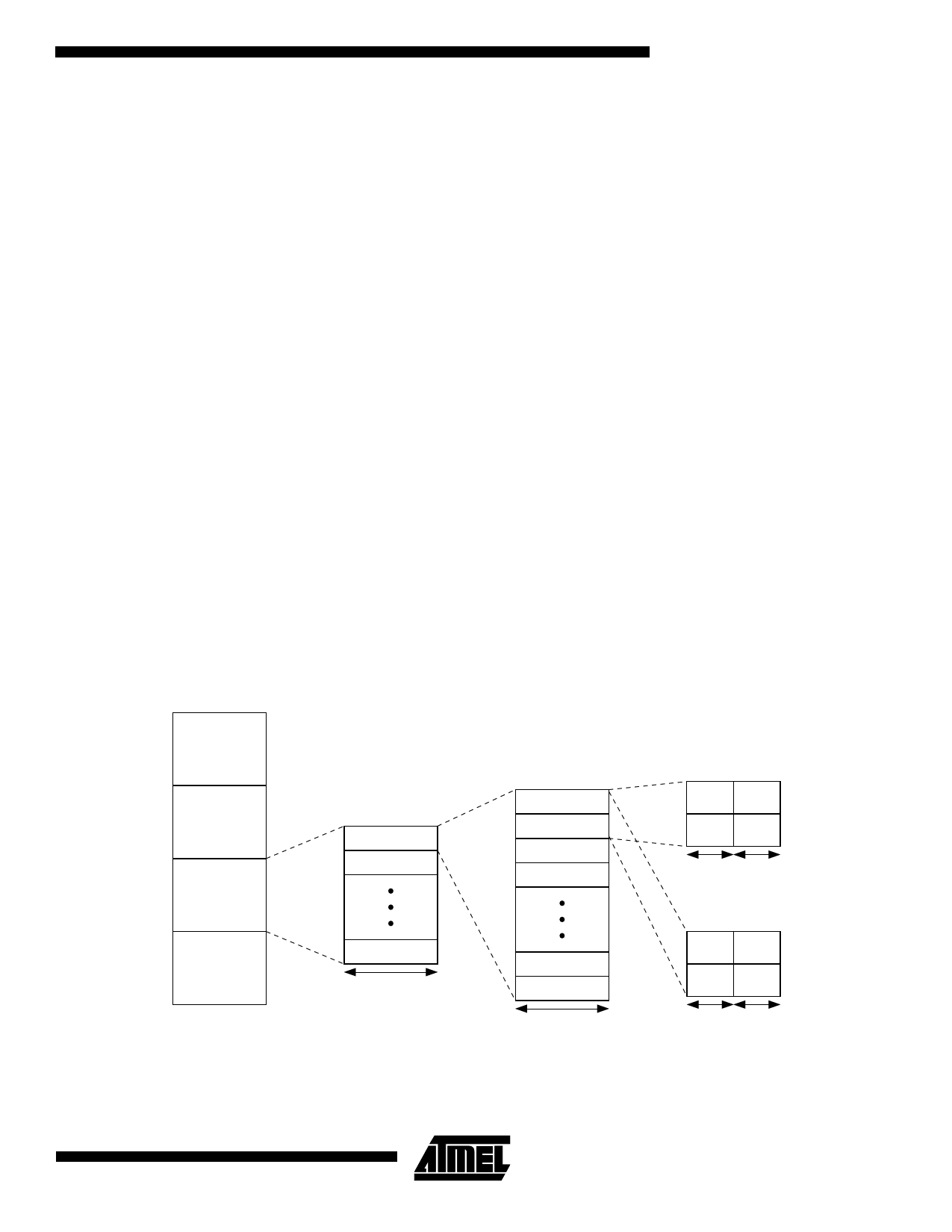
Figure 2. Memory Organization
32K x 16 SRAM
0000h
HSyncWidth, the width of active HSync in number of pixels.
VPeriod and VSyncWidth provide the same type of infor-
mation for VSync in terms of scan lines, rather than pixels.
These registers and others are used to control the video
interface of the chip. The other registers are HDelay, HAc-
tive, VDelay, and VActive. HDelay contains the number of
pixels between falling HSync and the first active pixel of a
line. HActive contains the number of active blocks in a line.
The size of the working memory depends on the size of the
image being processed. The external buffer should be
deep enough to store 16 scan lines of data at the highest
horizontal resolution. The equations for determining the
external buffer size are:
• Buffer bus width = 16 bits [For YUV data], 8 bits [For
Grayscale data]
• Buffer size = 16 x (No. of pixels per line)
As an example, a system designed to process images of
the maximum size of 1024 x 1024 pixels would have the
following external buffer requirements:
• Buffer size = 16 x 1024 = 16,384 words
Thus, this system would require 16K x 16 working memory
to process YUV images (color) and 16K x 8 working mem-
ory to process grayscale images. As the minimum size of
available SRAM is 32K x 8, the SRAM requirements are as
follows: YUV/grayscale images: two 32K x 8 SRAM’s to
form a 32K x 16 SRAM.
DATABANK A
2000h
NOT USED
4000h
DATABANK B
4000h
4400h
DATABANK B
SCAN LINE 1
SCAN LINE 2
000h
001h
002h
SCAN LINE
YU
YV
YU
YV
6000h
NOT USED
7FFFh
5C00h
SCAN LINE 8
1024 PIXELS
3FEh
3FFh
YU
YV
16 BITS
SRAM ORGANIZATION FOR MAXIMUM SCAN LINE SIZE OF 1024 PIXELS.
EACH DATABANK STORES 8 SCAN LINES OF THE RAW IMAGE.
AFTER COMPRESSION
Y
U
Y
V
8 BITS 8 BITS
AFTER DECOMPRESSION
U
Y
U
V
8 BITS 8 BITS
3
Share Link: 