W83194BR-640 Просмотр технического описания (PDF) - Winbond
Номер в каталоге
Компоненты Описание
Список матч
W83194BR-640 Datasheet PDF : 16 Pages
| |||
W83194BR-640
Clock Address
A(6:0) & R/W
Ack
8 bits dummy
Command code
Ack
8 bits dummy
Byte count
Ack
Byte0,1,2...
until Stop
Set R/W to 1 when read back the data sequence is as follows, [1101 0011] :
Clock Address
A(6:0) & R/W
Ack
Byte 0
Ack
Byte 1
Ack
Byte2, 3, 4...
until Stop
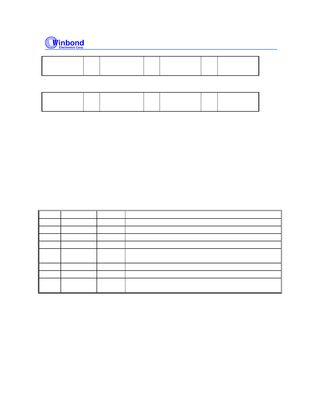
6.2 SERIAL CONTROL REGISTERS
The Pin column lists the affected pin number and the @PowerUp column gives the state at true power
up. Registers are set to the values shown only on true power up. "Command Code" byte and "Byte
Count" byte must be sent following the acknowledge of the Address Byte. Although the data (bits) in
these two bytes are considered "don't care", they must be sent and will be acknowledge. After that,
the below described sequence (Register 0, Register 1, Register 2, ....) will be valid and acknowledged.
6.2.1 Register 4: CPU Frequency Select Register (default = 0)
Bit @PowerUp
7
0
6
0
5
0
4
0
3
0
2
0
1
0
0
0
Pin
Description
-
SSEL3 (for frequency table selection by software via I2C)
-
SSEL2 (for frequency table selection by software via I2C)
-
SSEL1 (for frequency table selection by software via I2C)
-
SSEL0 (for frequency table selection by software via I2C)
-
0 = Selection by hardware
1 = Selection by software I2C - Bit 1,2, 7:4
-
SSEL4 (for frequency table selection by software via I2C)
-
SSEL5 (for frequency table selection by software via I2C)
-
0 = Running
1 = Tri-state all outputs
Publication Release Date: April. 2001
-7-
Revision 1.0
Share Link: 