W83194BR-640 Просмотр технического описания (PDF) - Winbond
Номер в каталоге
Компоненты Описание
Список матч
W83194BR-640 Datasheet PDF : 16 Pages
| |||
W83194BR-640
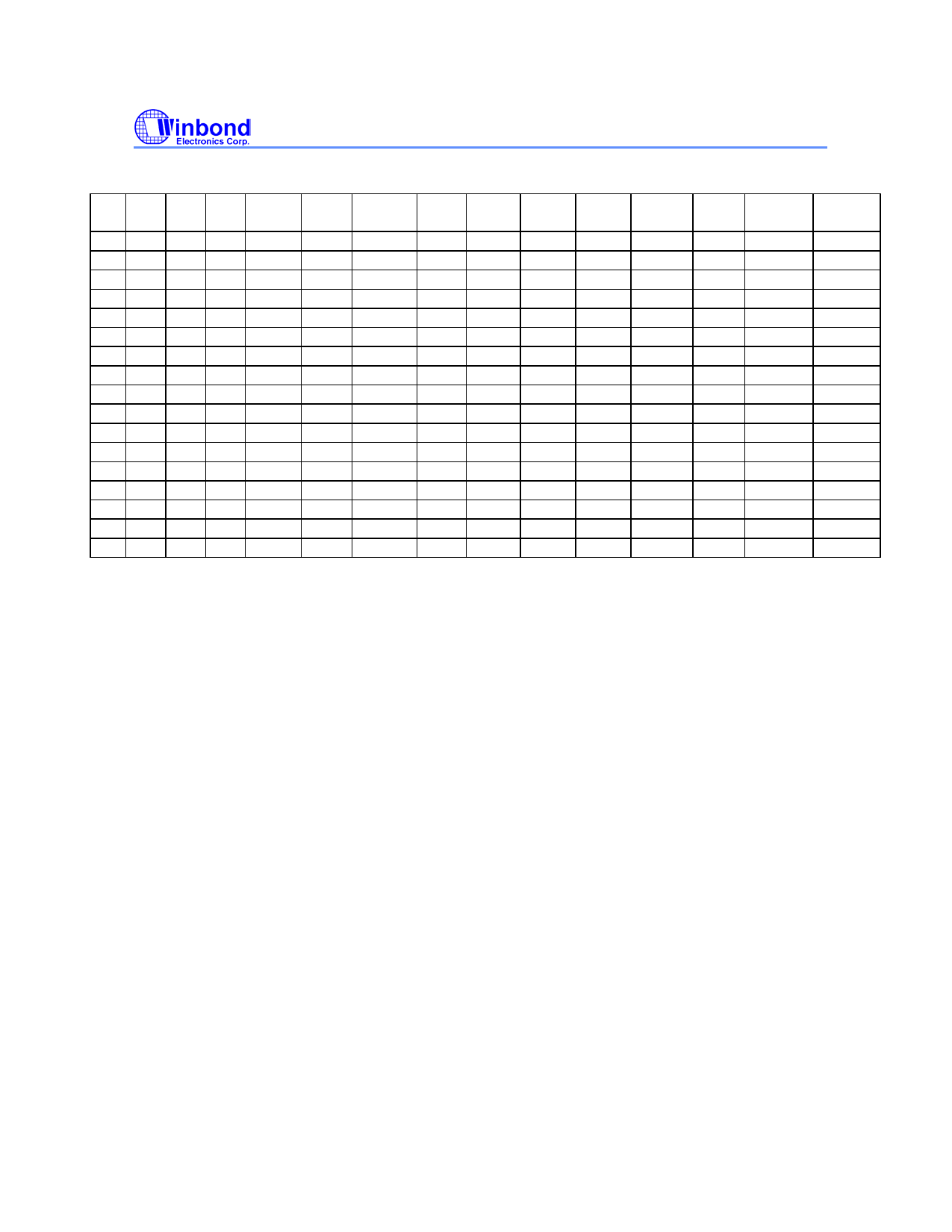
5. FREQUENCY SELECTION BY HARDWARE
VCO CPU SDRAM PCI AGP0 AGP1 CPU SDRAM PCI AGPSEL AGPSEL
=0
=1
FS3 FS2 FS1 FS0 (MHz) ratio ratio ratio ratio ratio (MHz) (MHz) (MHz) (MHz) (MHz)
0 0 0 0 399.6 6
6
2
6
8 66.6 66.6 33.3 66.6
50
0 0 0 1 400 4
4
3
6
8 100 100 33.3 66.6
50
0 0 1 0 498 3
3
5
8
10 166 166 33.2 62.5
50
0 0 1 1 399 3
3
4
6
8 133 133 33.3 66.6
50
0 1 0 0 399.6 6
4
2
6
8 66.6 100 33.3 66.6
50
0 1 0 1 400 4
6
3
6
8 100 66.6 33.3 66.6
50
0 1 1 0 400 4
3
3
6
8 100 133 33.3 66.6
50
0 1 1 1 399 3
4
4
6
8 133 100 33.3 66.6
50
1 0 0 0 336 3
3
3
5
6 112 112 37.3 67.2
56
1 0 0 1 372 3
3
4
6
8 124 124 31
62
46.5
1 0 1 0 414 3
3
4
6
8 138 138 34.5 69
51.8
1 0 1 1 300 2
2
5
5
6 150 150 30
60
50
1 1 0 0 399.6 6
3
2
6
8 66.6 133 33.3 66.6
50
1 1 0 1 498 4
3
4
8
10 124.5 166 31.13 62.5
50
1 1 1 0 300 2
3
5
5
6 150 100 30
60
50
1 1 1 1 480 3
4
5
8
10 160 120 32
60
48
6. FUNCTION DESCRIPTION
6.1 2-WIRE I2C CONTROL INTERFACE
The clock generator is a slave I2C component which can be read back the data stored in the latches
for verification. All proceeding bytes must be sent to change one of the control bytes. The 2-wire
control interface allows each clock output individually enabled or disabled. On power up, the
W83194BR-640 initializes with default register settings, and then it ptional to use the 2-wire control
interface.
The SDATA signal only changes when the SDCLK signal is low, and is stable when SDCLK is high
during normal data transfer. There are only two exceptions. One is a high-to-low transition on SDATA
while SDCLK is high used to indicate the beginning of a data transfer cycle. The other is a low-to-
high transition on SDATA while SDCLK is high used to indicate the end of a data transfer cycle. Data
is always sent as complete 8-bit bytes followed by an acknowledge generated.
Byte writing starts with a start condition followed by 7-bit slave address [1101 0010], command code
checking [0000 0000], and byte count checking. After successful reception of each byte, an
acknowledge (low) on the SDATA wire will be generated by the clock chip. Controller can start to
write to internal I2C registers after the string of data. The sequence order is as follows:
Bytes sequence order for I2C controller :
-6-
Publication Release Date: April. 2001
Revision 1.0
Share Link: 