W83194BR-640 Просмотр технического описания (PDF) - Winbond
Номер в каталоге
Компоненты Описание
Список матч
W83194BR-640 Datasheet PDF : 16 Pages
| |||
W83194BR-640
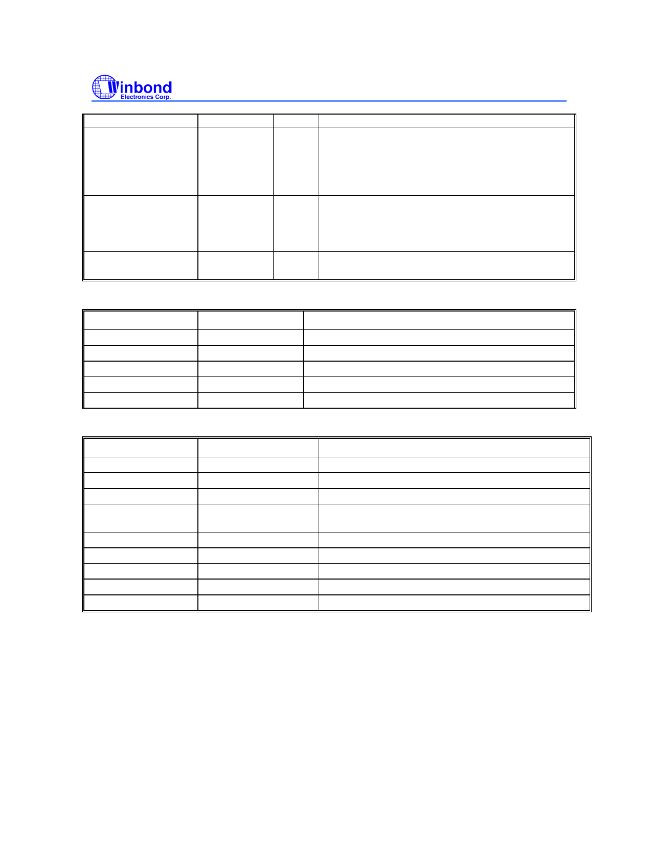
REF1^/&FS1
24_48MHz#/
&AGPSEL
48MHz ^
PCI clocks.
3
I/O 3.3V, 14.318MHz reference clock output. Internal
120kΩ pull-down.This pin has 1.5X drive strength.
Latched input for FS1 at initial power up for H/W
selecting the output frequency of CPU, SDRAM and
PCI clocks.
23
I/O 24MHz or 48MHz selected by Register.
AGPSEL at initial power up for H/W selecting the
output frequency of AGP clocks. Internal 120KΩ pull-
down.
22
O 48MHz output for USB. This pin has 1.5X drive
strength.
4.5 Power Management Pins
SYMBOL
PIN
AGP_STOP#
29
SDRAM_STOP#
30
PD#
31
CPU_STOP#
32
PCI_STOP#
33
FUNCTION
AGP clock stop control pin.
SDRAM clock stop control pin.
Power Down pin, if PD#=0, all clocks are stopped.
CPU clock stop control pin.
PCI clock stop control pin.
4.6 Power Pins
SYMBOL
VddR
VddAPIC
Vdd
VddC
VddAGP
VddP
VddSD
Vdd48
Vss
PIN
FUNCTION
1
Power supply for REF. 3.3V
48
Power supply for IOAPIC0, 2.5V.
25
Power supply for core logic. 3.3V
41,45
Power supply for CPUCLK1T and CPUCLK0T,
CPUCLK1T, IOAPIC0, 2.5V.
17
Power supply for AGP outputs.
11
Power supply for PCI outputs.
36
Power supply for SDRAM and 48/24MHz outputs.
21
Power supply for 48/24MHz outputs.
4,5,8,14,20,26,46,39,42 Circuit Ground.
Publication Release Date: April. 2001
-5-
Revision 1.0
Share Link: 