W83194BR-640 Просмотр технического описания (PDF) - Winbond
Номер в каталоге
Компоненты Описание
Список матч
W83194BR-640 Datasheet PDF : 16 Pages
| |||
W83194BR-640
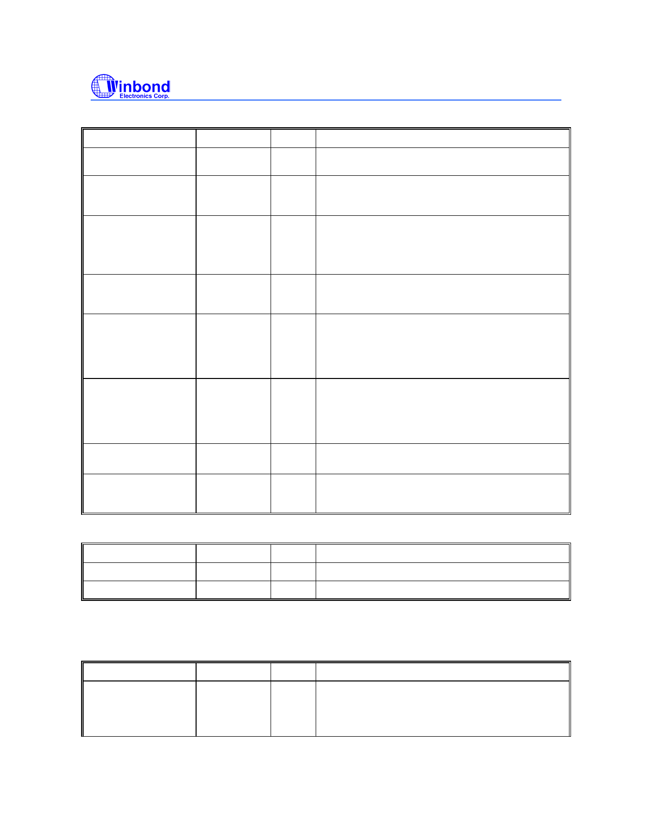
4.2 CPU, SDRAM, PCI Clock Outputs
SYMBOL
PIN
I/O
FUNCTION
IOAPIC0
CPUCLK0T
CPUCLK0C
CPUCLK1T
SDRAM_out
PCICLK_F^/ &FS2
PCICLK 1^/ &FS3
PCICLK ^[2:5]
RESET#
47
44,43
40
35
9
10
12,13,15,16
37
OUT
OUT
OUT
OUT
I/O
I/O
OUT
OD
16.7/33MHz APIC clock for CPU and Chipset by I2C
byte 7 bit 3
True CPU clock output and Complementary CPU
clock output. This pin will be stopped by
CPU_STOP#
Low skew (< 250ps) clock outputs for host
CPU clock output for chipset and CPU,
When byte 9 bit 6 = 0
This pin will not be stopped by CPU_STOP#
SDRAM clock output which have syn. or asyn.
Frequencies as CPU clocks. The clock phase is the
same as CPUCLK0T and CPUCLK1T.
Latched input for FS2 at initial power up for H/W
selecting the output frequency of CPU, SDRAM and
PCI clocks. Internal 120KΩ pull-down
PCI free running clock during normal operation.
PCI output has 1.5X drive strength.
Latched input for FS3 at initial power up for H/W
selecting the output frequency of CPU, SDRAM and
PCI clocks. Internal 120KΩ pull-down
PCI clock during normal operation.
PCI output has 1.5X drive strength.
Low skew (< 250ps) PCI clock outputs.
PCI outputs have 1.5X drive strength.
Open Drain, 4ms low active pulse when Watch Dog
time out, the all clock output recover to hardware
FS0-FS3 setting.
4.3 I2C Control Interface
SYMBOL
*SDATA
*SDCLK
PIN
I/O
FUNCTION
28
I/O Serial data of I2C 2-wire control interface
27
IN Serial clock of I2C 2-wire control interface
4.4 Fixed Frequency Outputs
SYMBOL
PIN
REF0^/&FS0
2
I/O
FUNCTION
I/O 3.3V, 14.318MHz reference clock output. Internal
120kΩ pull-down.This pin has 1.5X drive strength.
Latched input for FS0 at initial power up for H/W
selecting the output frequency of CPU, SDRAM and
Publication Release Date: April. 2001
-4-
Revision 1.0
Share Link: 