BS616UV2019(2004) Просмотр технического описания (PDF) - Brilliance Semiconductor
Номер в каталоге
Компоненты Описание
Список матч
BS616UV2019 Datasheet PDF : 9 Pages
| |||
BSI
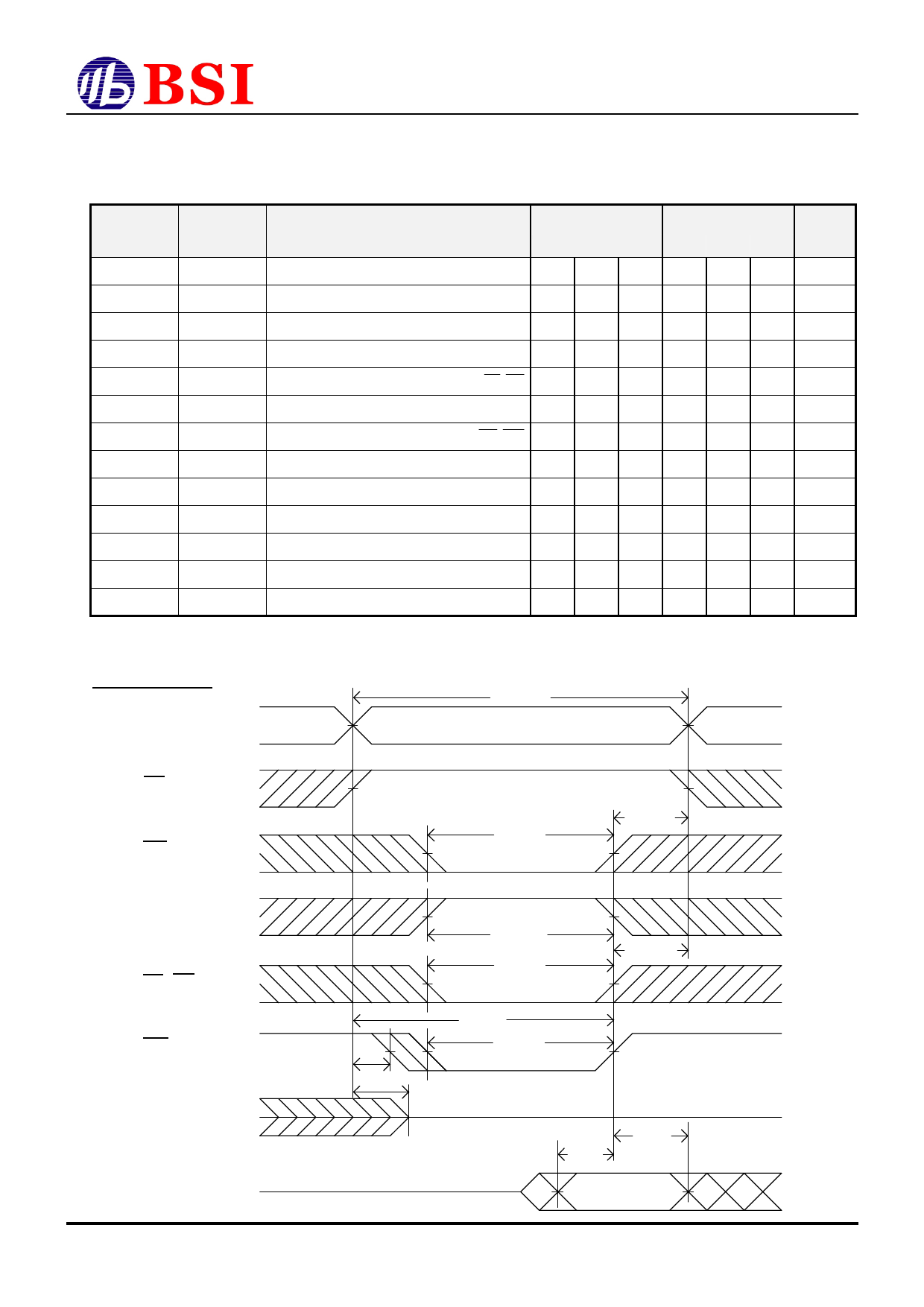
WRITE CYCLE2 (1,6)
ADDRESS
CE2
CE
LB,UB
WE
D OUT
D IN
BS616UV2019
t WC
(5,12)
(5)
(11)
t CW
t AS
t BW
(5)
t AW
(4,10)
t WHZ
t WP
(2)
t WR (3)
t OW
(7)
(8)
t DW
t DH
(8,9)
NOTES:
1. WE must be high during address transitions.
2. The internal write time of the memory is defined by the overlap of CE2, CE and WE low. All signals
must be active to initiate a write and any one signal can terminate a write by going inactive.
The data input setup and hold timing should be referenced to the second transition edge of
the signal that terminates the write.
3. TWR is measured from the earlier of CE2 going low, or CE or WE going high at the end of write cycle.
4. During this period, DQ pins are in the output state so that the input signals of opposite phase
to the outputs must not be applied.
5. If the CE2 high transition or CE low transition occurs simultaneously with the WE low transitions or after the WE
transition, output remain in a high impedance state.
6. OE is continuously low (OE = VIL ).
7. DOUT is the same phase of write data of this write cycle.
8. DOUT is the read data of next address.
9. If CE2 is high or CE is low during this period, DQ pins are in the output state. Then the data input signals of
opposite phase to the outputs must not be applied to them.
10. The parameter is guaranteed but not 100% tested.
11. TCW is measured from the later of CE2 going high or CE going low to the end of write.
12. 48B BGA ignore this parameters related to CE2 .
R0201-BS616UV2019
7
Revision 1.1
Jan. 2004
Share Link: 