BS616UV2019(2004) Просмотр технического описания (PDF) - Brilliance Semiconductor
Номер в каталоге
Компоненты Описание
Список матч
BS616UV2019 Datasheet PDF : 9 Pages
| |||
BSI
BS616UV2019
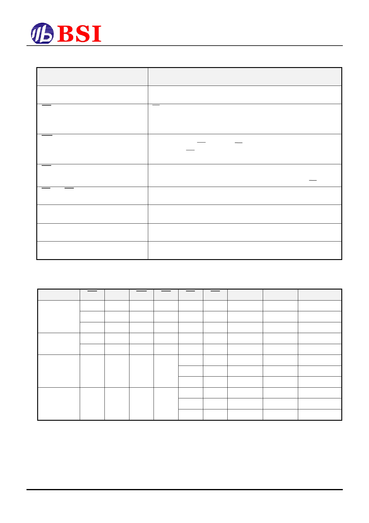
PIN DESCRIPTIONS
Name
A0-A16 Address Input
Function
These 17 address inputs select one of the 131,072 x 16-bit words in the RAM.
CE Chip Enable 1 Input
CE2 Chip Enable 2 Input
CE is active LOW and CE2 is active HIGH. Both chip enables must be active when
data read from or write to the device. If either chip enable is not active, the device is
deselected and is in a standby power mode. The DQ pins will be in the high
impedance state when the device is deselected. (48B BGA ignore CE2 pin)
WE Write Enable Input
OE Output Enable Input
LB and UB Data Byte Control Input
The write enable input is active LOW and controls read and write operations. With the
chip selected, when WE is HIGH and OE is LOW, output data will be present on the
DQ pins; when WE is LOW, the data present on the DQ pins will be written into the
selected memory location.
The output enable input is active LOW. If the output enable is active while the chip is
selected and the write enable is inactive, data will be present on the DQ pins and they
will be enabled. The DQ pins will be in the high impedance state when OE is inactive.
Lower byte and upper byte data input/output control pins.
DQ0 - DQ15 Data Input/Output
Ports
Vcc
These 16 bi-directional ports are used to read data from or write data into the RAM.
Power Supply
Gnd
Ground
TRUTH TABLE
MODE
CE
CE2 (1) WE
OE
LB UB
H
X
X
X
X
X
Not selected
(Power Down)
X
L
X
X
X
X
X
X
X
X
H
H
Output Disabled
L
H
H
H
X
X
L
L
Read
L
H
H
L
H
L
L
H
L
L
Write
L
H
L
X
H
L
L
H
1. 48B BGA ignore CE2 condition.
D0~D7
High Z
High Z
High Z
High Z
Dout
High Z
Dout
Din
X
Din
D8~D15
High Z
High Z
High Z
High Z
Dout
Dout
High Z
Din
Din
X
Vcc CURRENT
I , I CCSB CCSB1
I , I CCSB CCSB1
I , I CCSB CCSB1
ICC
ICC
ICC
ICC
ICC
ICC
ICC
R0201-BS616UV2019
2
Revision 1.1
Jan. 2004
Share Link: 