M65761FP Просмотр технического описания (PDF) - MITSUBISHI ELECTRIC
Номер в каталоге
Компоненты Описание
Список матч
M65761FP Datasheet PDF : 29 Pages
| |||
MITSUBISHI ICs (LSI)
M65761FP
QM-CODER
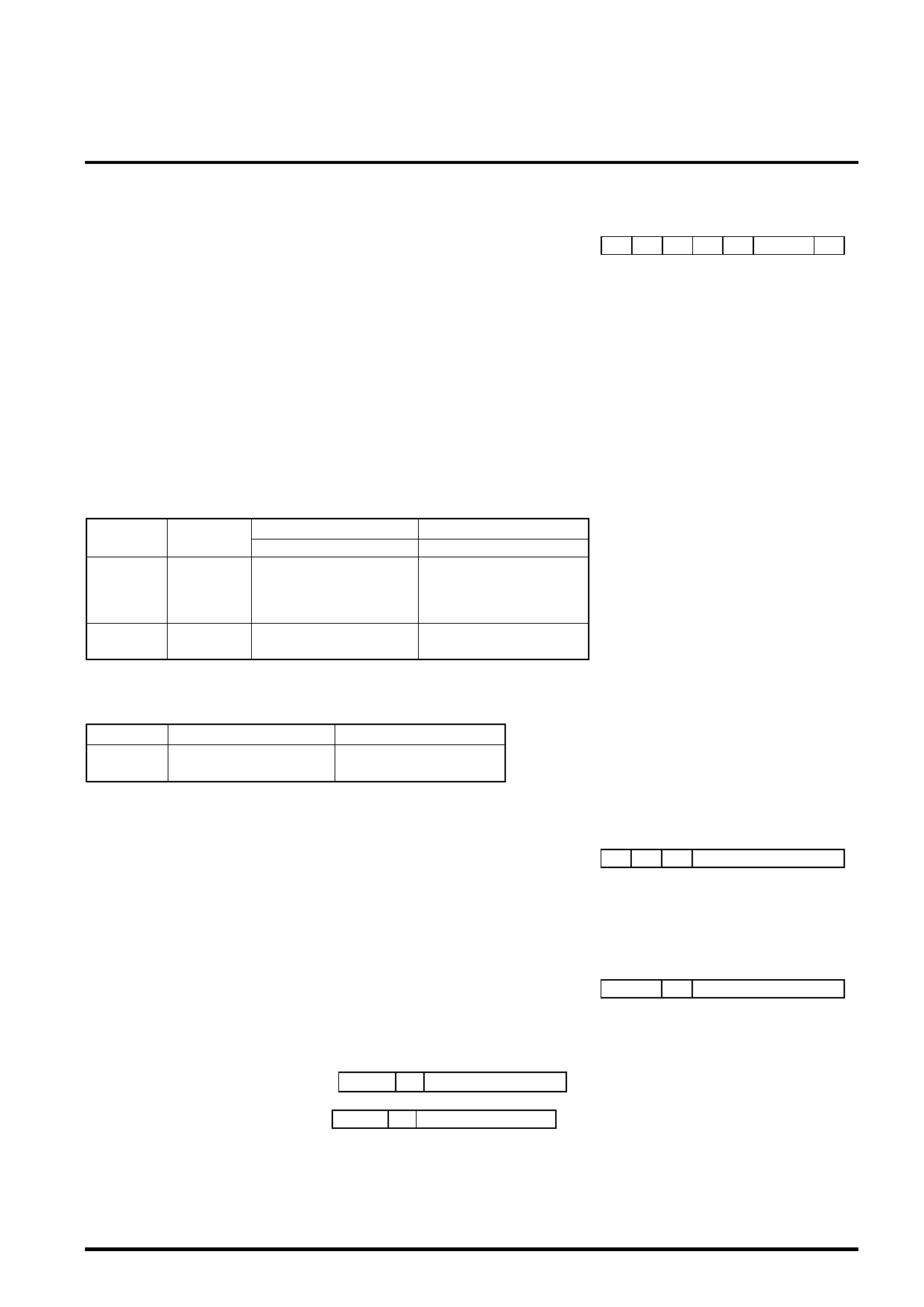
11. 2 Description of Registers
(1) System Set Up Register (W/R) (address : 0)
d0(HR) : H/W reset (0:Active, 1:Reset state)
To make a H/W reset ,set this bit to 1 then to 0.
d7(MSB)
d0
SYS_REG : PB PI BX BS CX MOD HR
Reset initializes the entire LSI including the group of register and Line Memory. However, the context table RAM is not
initialized.
d1-2(MOD) :This sets up the operating modes.
d3(CX)
(d2=0,d1=0:coding, d2=1,d1=0:iage data through (Iage data I/F→Host I/F),
d2=0,d1=1:decoding, d2=1,d1=1:Iage data through (Host I/F→Iage data I/F))
:Context select (0:internal context, 1:Image data through)
NOTE:The internal context should be selected when the image data through mode is used.
When initializing or processing R/W of the Context table RAM and coding /decoding,
This bit must be set the same.(Because RAM configration changes depending on internal/external modes.)
d4(BS) :Select data bit swap of the host bus. (0:MSB(d7)first, 1:LSB(d0)first)
d5(BX) :Select data byte swap of the host bus.(0:Lower byte(A)first, 1:Upper byte(B)first)
NOTE:BX is valid only when the host bus is 16 bits.(BUS16=HIGH)
Table 11. 2 The coed data and image data line-up on the Host bus
Bus width
BUS16
1
16bit
0
8bit
Swap
BX BS
00
01
10
11
–0
–1
Upper address(B)
d15 • • • • • • d8
b8 • • • • • • b15
b15 • • • • • • b8
b0 • • • • • • b7
b7 • • • • • • b0
–
–
Lower address(A)
d7 • • • • • • d0
b0 • • • • • • b7
b7 • • • • • • b0
b8 • • • • • • b15
b15 • • • • • • b8
b0 • • • • • • b7
b7 • • • • • • b0
b0 is the first coded data on the time
series/the left-hand side image data on the
screen.
b15 is the last coded data on the time
series/the right-hand image data on the
screen.
d6(PI) :Selects the image data I/O I/F (0:Serial /F, 1:ParallelI/F)
d7(PB) :Selects the bit width of the iamge data bus (0:32bit bus (PD0-31), 1:16bit bus(PD0-15))
Table 11. 3 The image data line-up on the image data parallel bus
bit width
PB=0
PB=1
PD31 • • • • • • PD16
p0 • • • • • • p15
–
PD15 • • • • • • PD0
p16 • • • • • • p31
p0 • • • • • • p15
p0 is the image data on the left-hand on the screen.
p31is the image data on the right-hand on the screen.
(2) Parameter Setup Register (W/R) (Address:1)
d7
d4
d0
1) External Context Mode
PARA_REG : C0 LC 0
0
d6 (LC) :Condition of taking in the input from the external context are selected.
(0:through onput, 1:latch input)
When this bit is set to 1,the CX0 to CX11 of the context input is latched once using the transfer clock.("XCLK")
d7 (C0) : When this bit is set to 1,CX0 is selected.
(0:CX0 external input, 1:CX0 internal feedback)
2) Internal Context Mode
d0-4 (AT<0>-AT<4>) :ATpixel position Lower 5bits. (See Fig.9. 2)
d7 d6 d5 d4
PARA_REG :
AT TM
d0
AT
d5 (TM) :Template select (0:3line template, 1:2line template)
d6 -7(AT<5>-AT<6>) :AT pixel position upper 2bits (the 6th and 7th bits)
d7
d4
d0
Example : 3line template,AT=4 :
0 0 0 0 0 1 00
d7
d4
d0
2line template,AT=48 : 0 1 1 1 0 0 0 0
NOTE) The AT pixel position at time of the internal context mode is set up by using all the AT<6:0> (0 to 127)
When the default position (when the AT pixels are not used) is used, At is set to 0.
When the 2-line templsate is used, AT should not be set to 1 to 4. In case of the 3-line template,
AT=1 to 2 is not allowed.
Share Link: 