M65761FP Просмотр технического описания (PDF) - MITSUBISHI ELECTRIC
Номер в каталоге
Компоненты Описание
Список матч
M65761FP Datasheet PDF : 29 Pages
| |||
MITSUBISHI ICs (LSI)
M65761FP
QM-CODER
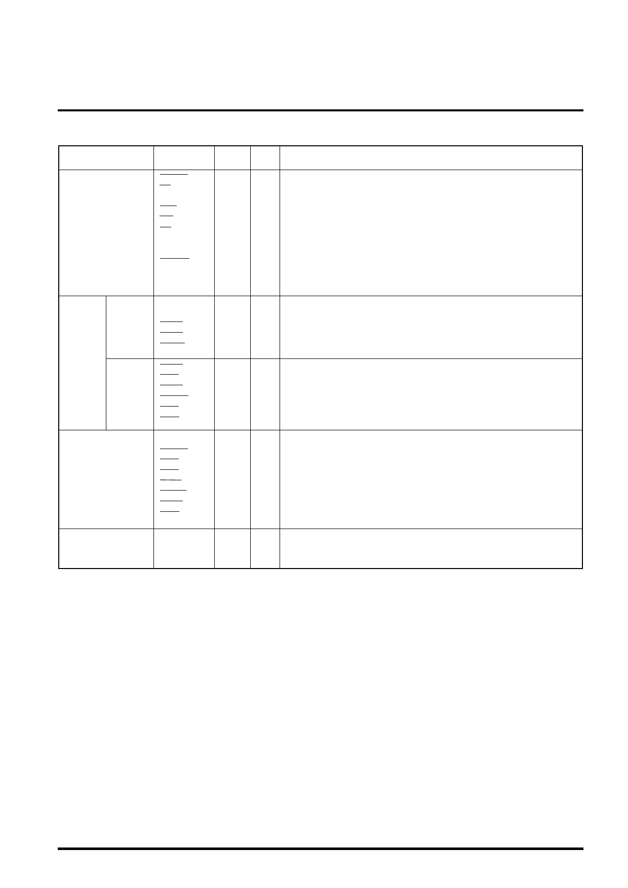
10. FUNCTIONAL DESCRIPTION OF PINS
Classification
Pin name
I/O BUF
Function
Host Bus I/F
RESET
CS
A0-3
BHE
WR
RD
D0-15
DMARQ
DMAAK
INTR
BUS16
I
S H/W reset signal
I
Chip select signal
I
Internal register address select signal
I
High-order(D8-15)access signal
I
S Write strobe signal
I
S Read strobe signal
IO
8 I/O data signal (D0-7 used on 8-bit bus)
O
2 Code data DMA request signal
I
US Code data DMA acknowledge signal
O
2 Interrupt request signal
I
U 8-bit bus (D0-7)and 16-bit bus(D0-15)function select bus.
Parallel
Image data
I/F
Serial
PD0-31
PDRQ
PDAK
PDRD
PDWR
PRDY
PTIM
PXCK
PXCKO
SVID
RVID
IO U2 Parallel image I/O bus (PD0-15 used on 16-bit bus)
O
2 Image data DMA request signal
I
US Image data DMA acknowledge signal
I
US Image data read strobe signal
I
US Image data write strobe signal
O
2 Image data 1-line I/O start ready signal
I
US Image data 1-line transfer section signal
I
US Image data transfer clock signal
O
4 Image data transfer sync clock signal
I
U Image data input signal
O
2 Image data output signal
Context I/F
CX0-11
PEUPE
SPIX
RPIX
XCLK
XWAIT
XRDY
XTIM
I
U Context input (CX0 can be fed back inside LSI)
(=PD0-11)
I
U PE RAM update enable (learning function ON/OFF) (=PD15)
I
U Coded image data input signal
(=SVID)
O
2 Decoded image data output signal
(=RVID)
O
4 Context data transfer clock signal
I
US Context data transfer wait signal
O
2 Context data 1-stripe I/O start ready signal
(=PRDY)
I
US Context data 1-stripe transfer section signal
(=PTIM)
Others
MCLK
TEST0-1
Vcc/GND
I
Master clock input signal
I
DS Test signal (should be connected to GND when normally used).
–
–
Power supply (+5V)/ground
Notes:Most of the context I/F signals are used in conjunction with the image data I/F signals.
∗ The input buffers of the input terminals (I and IO) are at TTL level.
Options are as follows.
(U:with pull-up resistors,D:with pull-down resistors,S:Schmitt trigger)
∗ Numbers (2,4,8) of the BUF column of the output terminals (O and IO) indicate current value. (one of 2,4,or 8mA)
Share Link: 