RV5C386A-E2 Просмотр технического описания (PDF) - RICOH Co.,Ltd.
Номер в каталоге
Компоненты Описание
Список матч
RV5C386A-E2 Datasheet PDF : 42 Pages
| |||
PRELIMINARY
RV5C386A
13.
13.1.
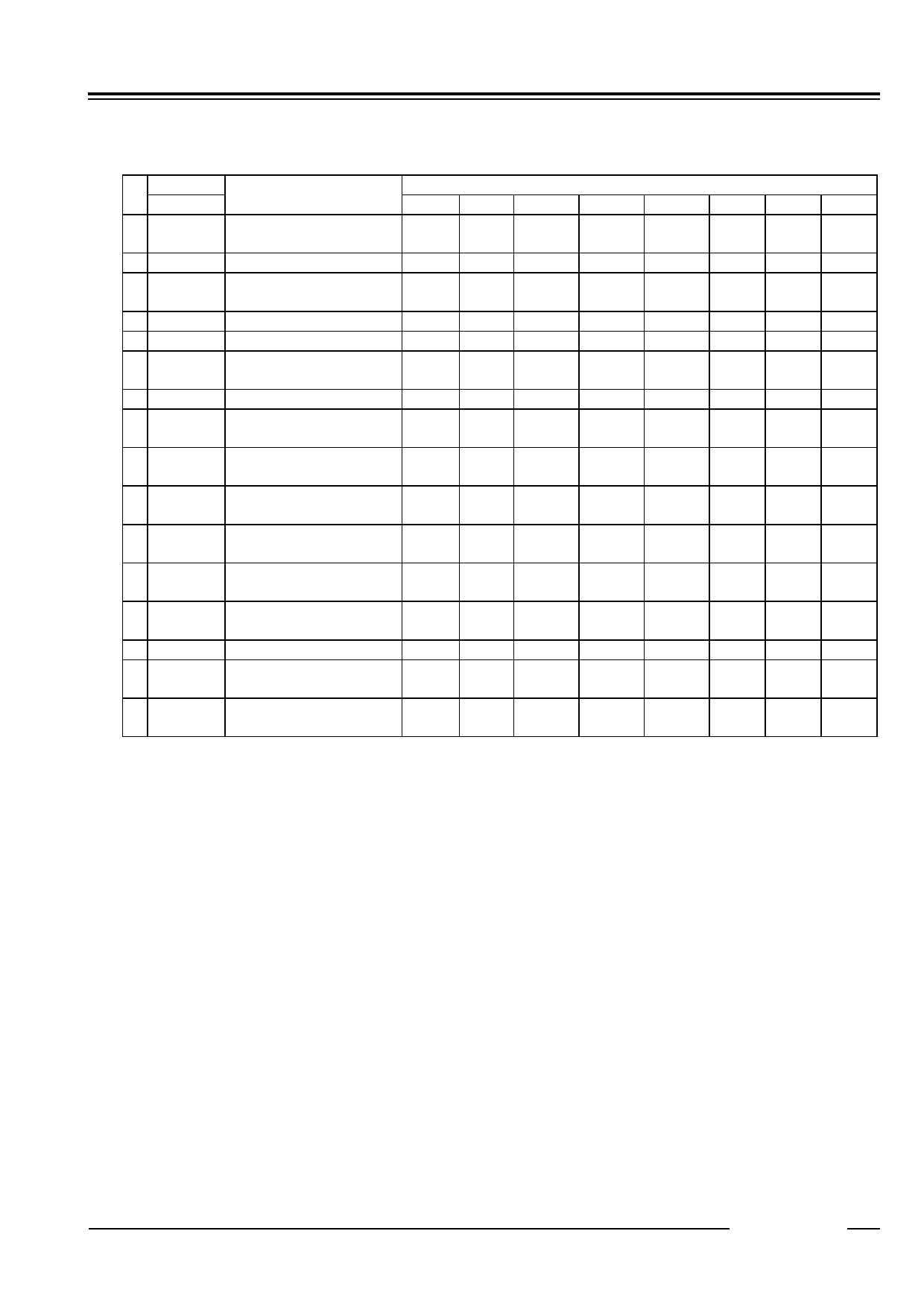
FUNCTION DESCRIPTIONS
Address Mapping
Address Register Name
A3A2A1A0
0 0 0 0 0 Second Counter
1 0 0 0 1 Minute Counter
2 0 0 1 0 Hour Counter
3 0 0 1 1 Day-of-week Counter
4 0 1 0 0 Day-of-month Counter
5 0 1 0 1 Month Counter and
Century Bit
6 0 1 1 0 Year Counter
7 0 1 1 1 Oscillation Adjustment
Register *3)
8 1 0 0 0 Alarm_W
(Minute Register)
9 1 0 0 1 Alarm_W
(Hour Register)
A 1 0 1 0 Alarm_W
(Day-of-week Register)
B 1 0 1 1 Alarm_D
(Minute Register)
C 1 1 0 0 Alarm_D
(Hour Register)
D 1101
E 1 1 1 0 Control Register 1 *3)
F 1 1 1 1 Control Register 2 *3)
D7 D6
- S40
*2)
- M40
-
-
-
-
-
-
/19⋅20 -
Data
D5
D4
S20 S10
M20 M10
H20 H10
P⋅/A
-
-
D20 D10
-
MO10
Y80 Y40 Y20 Y10
-
F6
F5
F4
- WM40 WM20 WM10
-
- WH20 WH10
WP⋅/A
- WW6 WW5 WW4
- DM40 DM20 DM10
-
-
-
-
WALE DALE
VDSL VDET
DH20
DP⋅/A
-
/12⋅24
SCRA-
TCH1
DH10
-
SCRA-
TCH3
XSTP
D3
S8
M8
H8
-
D8
MO8
Y8
F3
WM8
WH8
WW3
DM8
DH8
-
TEST
SCRA-
TCH2
D2 D1 D0
S4 S2 S1
M4 M2 M1
H4 H2 H1
W4
D4
MO4
W2
D2
MO2
W1
D1
MO1
Y4 Y2 Y1
F2 F1 F0
WM4 WM2 WM1
WH4 WH2 WH1
WW2 WW1 WW0
DM4 DM2 DM1
DH4 DH2 DH1
-
-
-
CT2 CT1 CT0
CTFG WAFG DAFG
Notes:
* 1) All the data listed above accept both reading and writing.
* 2) The data marked with "-" is invalid for writing and reset to 0 for reading.
* 3) When the XSTP bit is set to 1 in Control Register 2, all the bits are reset to 0 in Oscillation Adjustment
Register, Control Register 1 and Control Register 2 excluding the XSTP bit.
12345
-9-
Share Link: 