ZR36016 Просмотр технического описания (PDF) - Zoran Corporation
Номер в каталоге
Компоненты Описание
Список матч
ZR36016 Datasheet PDF : 36 Pages
| |||
Integrated Color Space / Raster-To-Block Converter
PXIN/PXOUT Bus Data Arrangement
The PXIN/PXOUT buses are 24 bits each. The 24 bits are
divided into 8-bit bytes, as follows.
MSB
LSB MSB
LSB MSB
LSB
PXIN/OUT[23:0]
23:16
15:8
7:0
The I/O arrangement is determined by the MODE and DSPY
fields, as shown below in Table 9. In this table, the 3 compo-
nents of (4:4:4), (4:2:2), (4:1:1), (1:0:0) formats are designated
(A:B:C), components of (4:4:4:4) format are designated
(A:B:C:D), and (A:B:C) corresponds with (R:G:B), (Y:Cb:Cr) or
(Cy:Ma:Ye). 1st, 2nd, etc., refer to the PXCLK time slots.
Table 9: I/O Bus Arrangements
PXINOUT
Bus
23-16
15-8
7-0
4:4:4
1st
2nd
A
A
B
B
C
C
4:2:2
1st
2nd
A
A
B
C
–
–
1st
A
B[7:6]
/C[7:6]
–
I/O Format
4:1:1
2nd
3rd
A
A
B[5:4]
/C[5:6]
B[3:2]
/C[3:2]
–
–
4th
A
B[1:0]
/C[1:0]
–
1:0:0
1st
2nd
A
A
–
–
–
–
4:4:4:4
1st
2nd
A
C
B
D
–
–
4:1:1 in Table 9 is the Philips H4V1 format. As shown in
Table 10, it uses only the upper 12-bits on the PXIN/PXOUT
buses.
Table 10: Philips 4:1:1 Format
PXIN/OUT
PXIN/OUT[23:16]
PXIN/OUT[15]
PXIN/OUT[14]
PXIN/OUT[13]
PXIN/OUT[12]
PXIN/OUT[11:0]
1st
A[7:0]
B[7]
B[6]
C[7]
C[6]
–
2nd
A[7:0]
B[5]
B[4]
C[5]
C[4]
–
3rd
A[7:0]
B[3]
B[2]
C[3]
C[2]
–
4th
A[7:0]
B[1]
B[0]
C[1]
C[0]
–
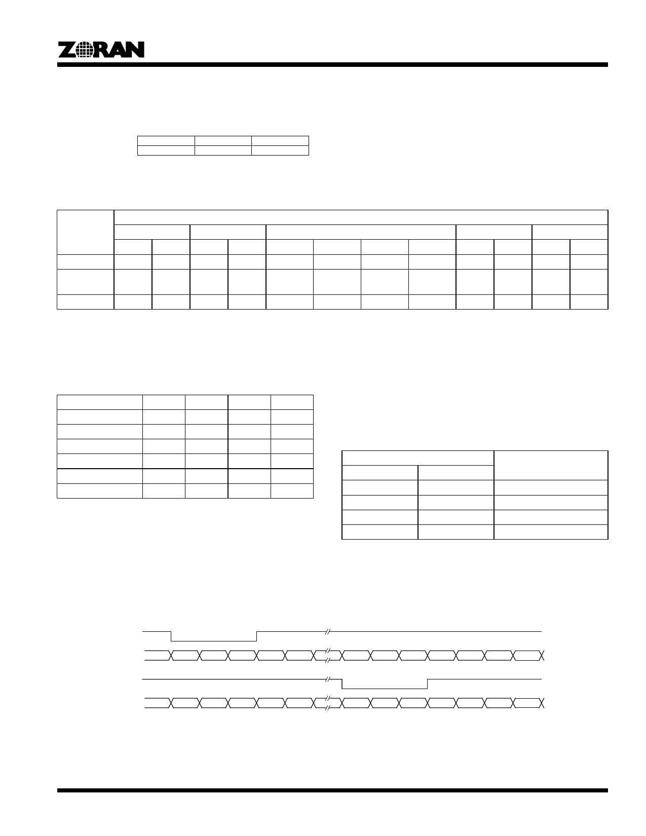
PXIN/PXOUT Delay
The image data which is input on the PXIN bus is output on the
PXOUT bus after an internal delay which depends on the MODE
field and HORZ bit of the registers. The delays of VIN to VOUT
and HIN to HOUT are the same as these. See Table 11 and
Figure 5.
Table 11: PXIN to PXOUT Delay
Configuration
MD [1]
HORZ
Delay in PXCLK Clock
Cycles (d)
0
0
20
0
1
24
1
0
17
1
1
20
1. Where MD = 1 when MODE = 0x0, 0x4, 0x8 or 0xC and = 0 for all others.
HIN
PXIN n-3
n-2
n-1
n
0
1
d-3
d-2
d-1
d
d+1
d+2
d+3
HOUT
PIXOUT n-3-d n-2-d n-1-d
n-d
-d
1-d
n = number of PXCLKs in one full line (HSYNC to HSYNC)
n-2
n-1
n
0
1
2
3
Figure 5. PXIN/PXOUT Delay Timing
11
Share Link: 