CDP1851 Просмотр технического описания (PDF) - Intersil
Номер в каталоге
Компоненты Описание
Список матч
CDP1851 Datasheet PDF : 14 Pages
| |||
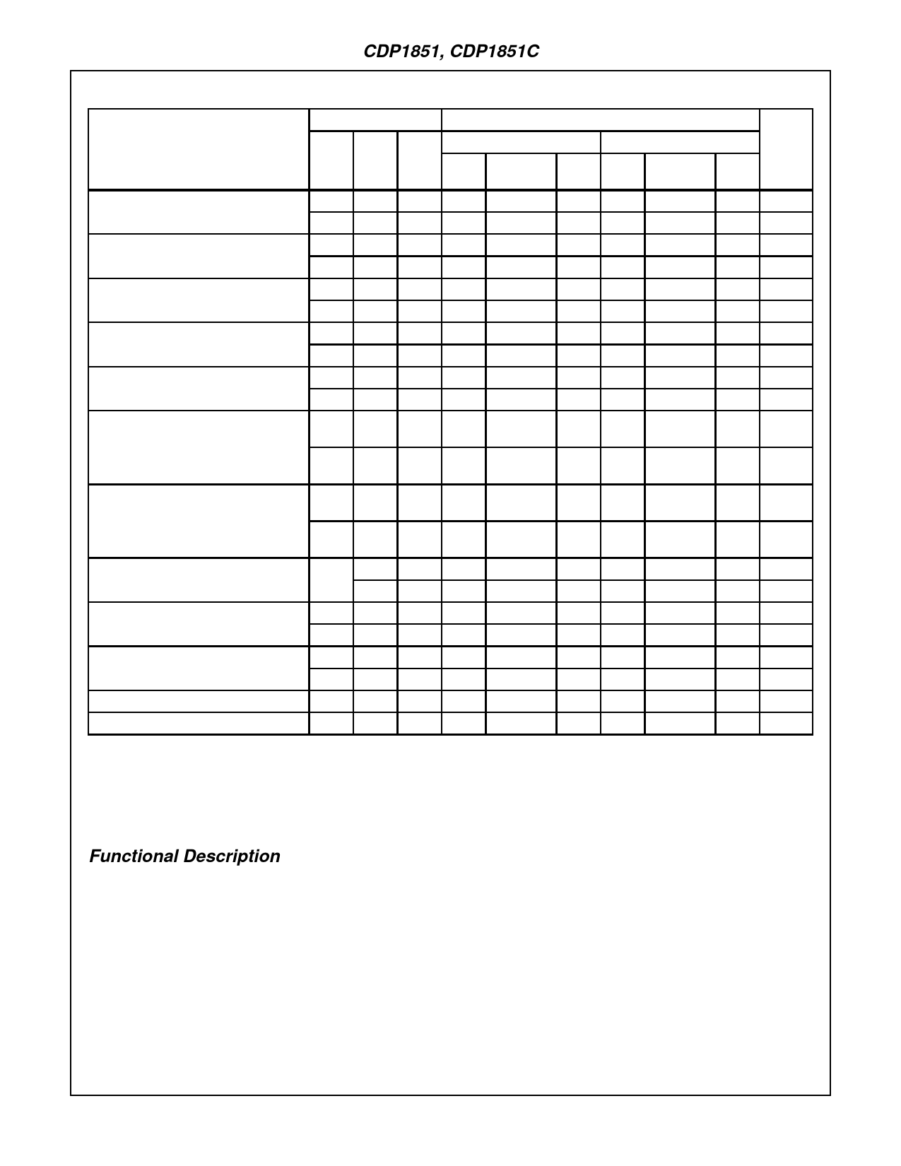
CDP1851, CDP1851C
Static Electrical Specifications At TA = -40oC to +85oC, VDD 5%, Unless Otherwise Specified
CONDITIONS
LIMITS
CDP1851
CDP1851C
PARAMETER
VO
VIN
VDD
(NOTE1)
(NOTE1)
(V) (V) (V) MIN
TYP
MAX MIN
TYP
MAX UNITS
Quiescent Device Current
IDD
-
0, 5
5
-
- 0, 10 10
-
0.01
50
-
1
200
-
0.02
200
µA
-
-
µA
Output Low Drive
(Sink) Current
IOL
0.4
0, 5
5
1.6
3.2
0.5 0, 10 10 2.6
5.2
-
1.6
3.2
-
-
-
-
mA
-
mA
Output High Drive
(Source) Current
IOH 4.6 0, 5
5 -1.15
-2.3
9.5 0, 10 10 -2.6
-5.2
- -1.15
-2.3
-
-
-
-
mA
-
mA
Output Voltage Low-Level
(Note 2)
VOL
-
0, 5
5
-
- 0, 10 10
-
0
0.1
-
0
0.1
-
0
0.1
V
-
-
V
Output Voltage High Level
VOH
-
0, 5
5
4.9
5
(Note 2)
- 0, 10 10 9.9
10
-
4.9
5
-
-
-
-
V
-
V
Input Low Voltage
VIL 0.5,
-
5
-
4.5
-
1.5
-
-
1.5
V
0.5,
-
10
-
-
3
-
-
-
V
9.5
Input High Voltage
VlH 0.5,
-
5
3.5
-
4.5
-
3.5
-
-
V
0.5,
-
10
7
-
-
-
-
-
V
9.5
Input Leakage Current
IlN
Any 0, 5
5
-
Input 0, 10 10
-
-
±1
-
-
±2
-
-
±1
µA
-
-
µA
Three-State Output Leakage
IOUT 0, 5 0, 5
5
-
Current
0, 10 0, 10 10
-
-
±1
-
-
±1
-
-
±1
µA
-
-
µA
Operating Current (Note 3)
IDD1
-
0, 5
5
-
1.5
3
-
1.5
3
mA
- 0, 10 10
-
6
12
-
-
-
mA
Input Capacitance
CIN
-
-
-
-
5
7.5
-
5
7.5
pF
Output Capacitance
COUT
-
-
-
-
10
15
-
10
15
pF
NOTES:
1. Typical values are for TA = 25oC and nominal VDD.
2. IOL = IOH = 1µA
3. Operating current is measured at 200kHz for VDD = 5V and 400kHz for VDD = 10V, with open output (worst-case frequencies for
CDP1802A system operating at maximum speed of 3.2MHz).
Functional Description
The CDP1851 has four modes of operation: input, output,
bidirectional, and bit-programmable. Port A is programmable
in all modes; port B is programmable in all but the
bidirectional mode. A control byte must be loaded into the
control register to program the ports. In the input and output
modes, each port has two handshaking signals, STROBE
and RDY. In the bidirectional mode, port A has four
handshaking signals: A RDY and A STROBE for input, B
RDY and B STROBE for output. If port A is programmed in
the bidirectional mode, port B must be programmed in the
bit-programmable mode. Each terminal of port A or B may
be individually programmed for input or output in the bit-
programmable mode. Since handshaking is not used in this
mode, the RDY and STROBE lines may also be used for bit-
programming if port A is not in the bidirectional mode.
Input Mode
When a peripheral device has data to input, it sends a
STROBE pulse to the PlO. The leading edge of this pulse
clears the RDY line, inhibiting further transmission from the
peripheral. The trailing edge of the STROBE pulse latches the
data into the PlO buffer register and also activates the INT line
to signal the CPU to read this data. The lNT pin can be wired
to the INT pin of the CPU or the EF lines for polling. The CPU
4-7
Share Link: 