M25P10 Просмотр технического описания (PDF) - STMicroelectronics
Номер в каталоге
Компоненты Описание
Список матч
M25P10 Datasheet PDF : 21 Pages
| |||
M25P10
Table 7. Status Register Format
b7
b0
SRWD 0 0 0 BP1 BP0 WEL WIP
Note: 1. SRWD, BP0 and BP1 are non-volatile read and write bits.
2. WEL and WIP are volatile read-only bits (WEL is set and
reset by specific instructions; WIP is automatically set
and reset by the internal logic of the device).
internally taken into account if, and only if, (BP0,
BP1) = (0,0).
SRWD bit: The SRWD bit operates together with
the W pin. SRWD bit and W pin allow the part to
be put in the Hardware protected mode. In this
mode (W pin = 0 and SRWD = 1), the non-volatile
bits of the Status Register (SRWD, BP1, BP0)
become read only bits and the Write Status
Register (WRSR) instruction has no more effect
on the device (please see the section entitled
“Write Protect (W)” on page 2, and Table 3).
Write in the Status Register (WRSR)
Prior to any WRSR instruction, a write enable
instruction (WREN) must have been previously
sent (the S input driven low, WREN instruction
properly transmitted and the S input driven high).
After the WREN instruction decoding, the memory
sets the Write Enable Latch (WEL) which allows
the execution of any further WRSR instruction.
The WRSR instruction is entered by driving the
Chip select input (S) low, followed by the
instruction byte and the data byte on Data In input
(D). WRSR instruction has no effect on b6, b5, b4,
b1 and b0 of the Status Register. b6, b5 and b4 are
always read at ’0’.
The device must be deselected just after the
eighth bit of the data byte has been latched in. If
not, the WRSR instruction is not executed. As
soon as the device is deselected, the self-timed
Write Status Register cycle (tW) is initiated. While
the Write Status Register cycle is in progress, the
Status Register may still be read to check the WIP
bit value. WIP is high during the self-timed Write
Status Register cycle and is low when it is
completed. When the cycle is completed, the write
enable latch (WEL) is reset.
The WRSR instruction allows the user to define
the size of the software Protected area (Read
Only) when setting the BP1,BP0 values, according
to Table 4. The WRSR instruction also allows the
user to set or reset the SRWD bit in accordance
with the W pin. SRWD bit and W pin allow the part
to be put in the Hardware protected mode (please
see the sections entitled “Read Status Register
(RDSR)” on page 8, “Write Protect (W)” on page 2,
and Table 3). WRSR instruction has no effect on
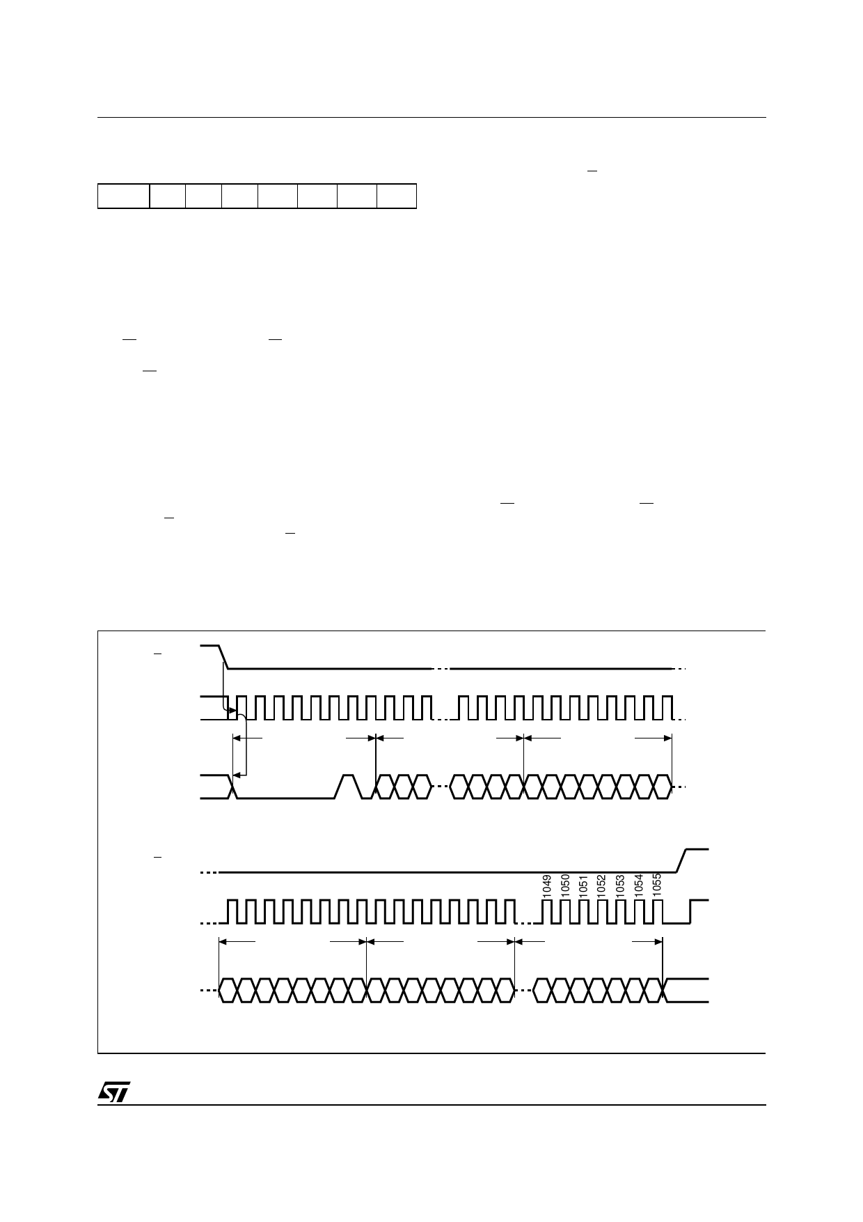
Figure 12. PP: Page Program Sequence
S
0 1 2 3 4 5 6 7 8 9 10 28 29 30 31 32 33 34 35 36 37 38 39
C
INSTRUCTION
24 BIT ADDRESS
DATA BYTE 1
D
23 22 21 3 2 1 0 7 6 5 4 3 2 1 0
S
40 41 42 43 44 45 46 47 48 49 50 51 52 53 54 55
C
DATA BYTE 2
DATA BYTE 3
DATA BYTE 128
D
7654321076543210
6543210
Note: 1. Address bits A23 to A17 are Don’t Care on the M25P10 series.
AI03749
9/21
Share Link: 