M25P10 Просмотр технического описания (PDF) - STMicroelectronics
Номер в каталоге
Компоненты Описание
Список матч
M25P10 Datasheet PDF : 21 Pages
| |||
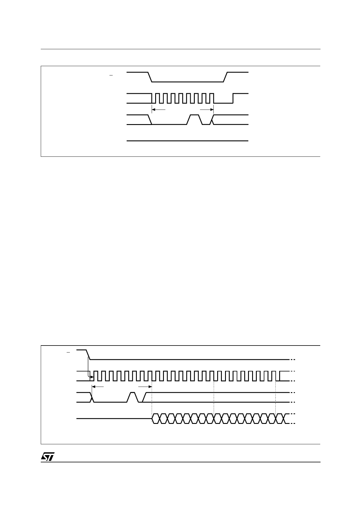
Figure 8. WRDI: Reset Write Enable Latch Sequence
S
01234567
C
INSTRUCTION
D
HIGH IMPEDANCE
Q
AI03750
M25P10
If more than 128 bytes are sent to the device,
previously latched data are discarded and the last
128 data bytes are guaranteed to be programmed
correctly within the same page. If less than 128
Data bytes are sent to device; they are correctly
programmed at the requested addresses without
having any effects on the other bytes of the same
Page.
The device must be deselected just after the
eighth bit of the last data byte has been latched in.
If not, the Page Program instruction is not
executed. As soon as the device is deselected, the
self-timed Page Program cycle (tPP) is initiated.
While the Page Program cycle is in progress, the
status register may be read to check the WIP bit
value. WIP is high during the self-timed Page
Program cycle and is low when it is completed.
When the cycle is completed, the write enable
latch (WEL) is reset.
A Page Program instruction applied to a Page
which is software protected by the BPi bits (see
Table 4 and Table 5) is not initiated.
The timing sequence is shown in Figure 12.
Write Enable (WREN) and Write Disable (WRDI)
The Write Enable Latch must be set prior to every
Page Program (PP), Sector Erase (SE), Bulk
Erase (BE) and Write Status Register (WRSR)
operation. The WREN instruction, whose timing
sequence is shown in Figure 7, will set the latch
and the WRDI instruction, whose timing sequence
is shown in Figure 8, will reset the latch.
The Write Enable Latch is reset under the
following conditions:
– Power on
– WRDI instruction completion
– WRSR instruction completion
– Page Program instruction completion
– Sector Erase instruction completion
– Bulk Erase instruction completion.
After completion of either WREN or WRDI
instruction, the chip enters a wait state and waits
for a deselect.
Figure 9. RDSR: Read Status Register Sequence
S
0 1 2 3 4 5 6 7 8 9 10 11 12 13 14 15
C
INSTRUCTION
D
STATUS REG. OUT
STATUS REG. OUT
HIGH IMPEDANCE
Q
76543210765432107
MSB
MSB
MSB
AI02031
7/21
Share Link: 