M25P10 Просмотр технического описания (PDF) - STMicroelectronics
Номер в каталоге
Компоненты Описание
Список матч
M25P10 Datasheet PDF : 21 Pages
| |||
M25P10
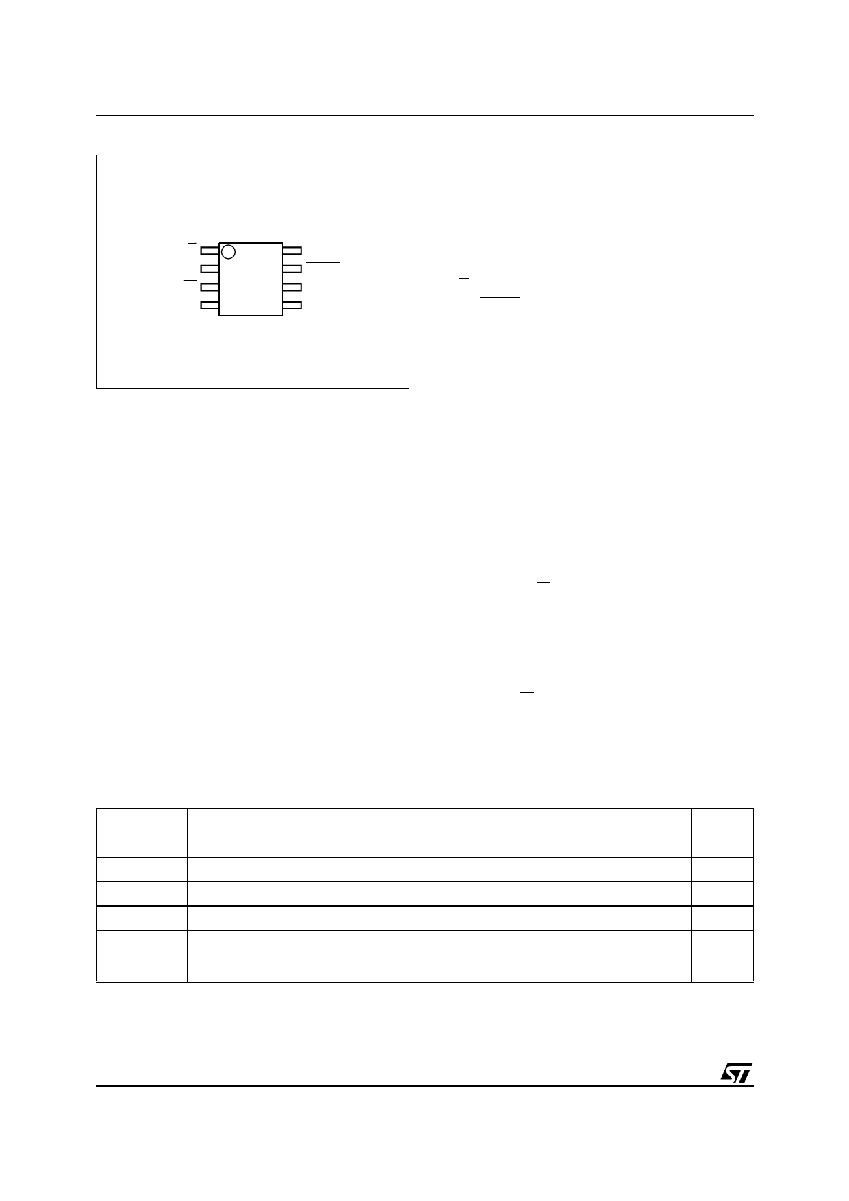
Figure 2. SO Connections
S
Q
W
VSS
M25P10
1
8
2
7
3
6
4
5
AI03745
VCC
HOLD
C
D
is clocked out during the high to low transition of
clock C
SIGNALS DESCRIPTION
Serial Output (Q)
The output pin is used to transfer data serially out
of the memory. Data is shifted out on the falling
edge of the serial clock.
Serial Input (D)
The input pin is used to transfer data serially into
the device. It receives instructions, addresses,
and the data to be programmed. Input is latched
on the rising edge of the serial clock.
Serial Clock (C)
The serial clock provides the timing of the serial
interface. Instructions, addresses, or data present
at the input pin are latched on the rising edge of
the clock input, while data on the Q pin changes
after the falling edge of the clock input.
Chip Select (S)
When S is high, the memory is deselected and the
Q output pin is at high impedance and, unless an
internal Read, Program, Erase or Write Status
Register operation is underway, the device will be
in the Standby Power mode (this is not the Deep
Power Down mode). S low enables the memory,
placing it in the active power mode. It should be
noted that after power-on, a high to low transition
on S is required prior to the start of any operation.
Hold (HOLD)
The HOLD pin is used to pause serial
communications with a SPI memory without
resetting the serial sequence. To take the Hold
condition into account, the product must be
selected. The HOLD condition is validated by a 0
state on the Hold pin synchronized with the 0 state
on the Clock, as shown in Figure 4. The DeHOLD
condition is validated by a 1 state on the Hold pin
synchronized with the 0 state on the Clock. During
the Hold condition D, Q, and C are at a high
impedance state.
When the memory is under HOLD condition, it is
possible to deselect the device. Then, the protocol
is reset. The memory remains on HOLD as long as
the Hold pin is Low. To restart communication with
the device, it is necessary to both DeHOLD (H =
1) and to SELECT the memory.
Write Protect (W)
This pin is for hardware write protection of the
Status Register (SR); except WIP and WEL bits.
When bit 7 (SRWD) of the status register is 0 (the
initial delivery state); it is possible to write the SR
once the WEL (Write Enable Latch) has been set
with the WREN instruction and whatever is the
status of pin W (high or low).
Table 2. Absolute Maximum Ratings 1
Symbol
Parameter
Value
Unit
TA
Ambient Operating Temperature
–40 to 85
°C
TSTG
Storage Temperature
–65 to 150
°C
TLEAD
Lead Temperature during Soldering
SO8: 40 seconds
215
°C
VIO
Input and Output Voltage Range (with respect to Ground)
–0.3 to 5.0
V
VCC
Supply Voltage Range
–0.6 to 5.0
V
VESD
Electrostatic Discharge Voltage (Human Body model) 2
2000
V
Note: 1. Except for the rating “Ambient Operating Temperature Range”, stresses above those listed in this table may cause permanent
damage to the device. These are stress ratings only, and operation of the device at these or any other conditions above those
indicated in the Operating sections of this specification is not implied. Exposure to Absolute Maximum Rating conditions for
extended periods may affect device reliability. Refer also to the ST SURE Program and other relevant quality documents.
2. MIL-STD-883C, 3015.7 (100 pF, 1500 Ω)
2/21
Share Link: 