M25P10 Просмотр технического описания (PDF) - STMicroelectronics
Номер в каталоге
Компоненты Описание
Список матч
M25P10 Datasheet PDF : 21 Pages
| |||
M25P10
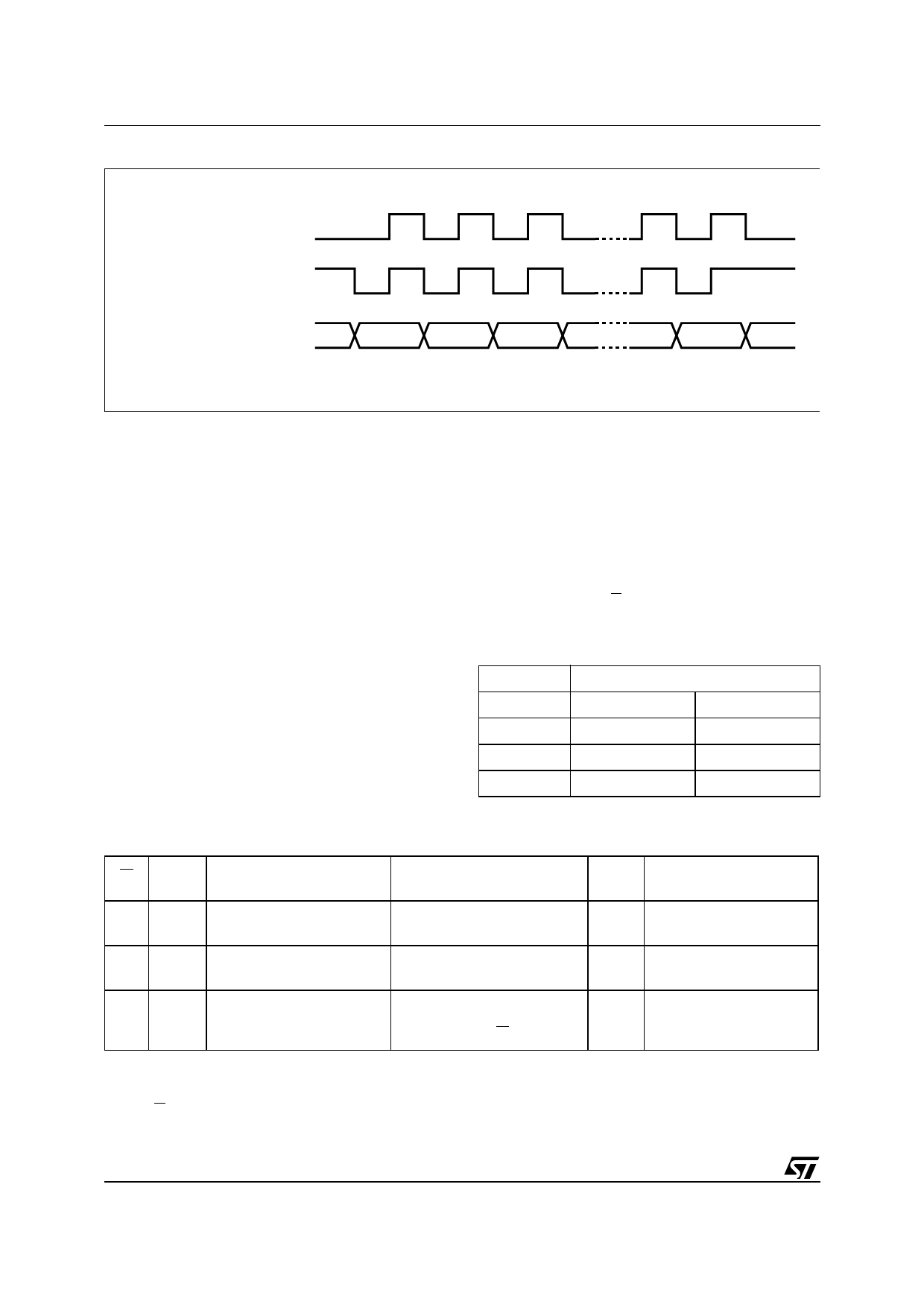
Figure 5. M25P10-Compatible SPI Modes
CPOL CPHA
0
0
C
1
1
C
D or Q
MSB
LSB
AI01438
Clock Polarity (CPOL) and Clock Phase
(CPHA) with SPI Bus
As shown in Figure 5, the M25P10 can be driven
by a microcontroller with its SPI peripheral running
in either of the two following modes: (CPOL,
CPHA) = (’0’, ’0’) or (CPOL, CPHA) = (’1’, ’1’). For
these two modes, input data is latched in by the
low to high transition of clock C, and output data is
available from the high to low transition of Clock
(C).The difference between (CPOL, CPHA) = (0,
0) and (CPOL, CPHA) = (1, 1) is the clock polarity
when in stand-by: C remains at ’0’ for (CPOL,
CPHA) = (0, 0) and C remains at ’1’ for (CPOL,
CPHA) = (1, 1) when there is no data transfer.
MEMORY ORGANIZATION
The memory is organized in 131,072 words of 8
bits each. The device features 1,024 pages of 128
bytes each. Each page can be individually
programmed (bits are programmed from ‘1’ to ’0’
state).
The device is also organized in 4 sectors of
262,144 bits (32,768 x 8 bits) each.The device is
Sector or Bulk Erasable but not Page Erasable
(bits are erased from ’0’ to ’1’ state).
OPERATIONS
All instructions, addresses and data are shifted in
and out of the chip MSB first. Data input (D) is
sampled on the first rising edge of clock (C) after
the chip select (S) goes low. Prior to any
Table 4. Memory Organization
Sector
Address Range
3
18000h
1FFFFh
2
10000h
17FFFh
1
08000h
0FFFFh
0
00000h
07FFFh
Table 3. Protection Features
W SRWD
Status Register (SR)
Data Bytes (Software
Protected Area by BPi bits)
Mode
Data Bytes (Unprotected
Area)
X
0
Writeable after setting WEL
Software protected by the BPi
bits of the Status Register
SPM
Paged Programmable and
Sector Erasable
1
1
Writeable after setting WEL
Software protected by the BPi
bits of the Status Register
SPM
Paged Programmable and
Sector Erasable
0
1
Hardware protected
Hardware protected by the
BPi bits of the Status Register
and the W pin
HPM
Note: 1. SPM: Software Protected Mode.
2. HPM: Hardware Protected Mode.
3. BPi: Bits BP0 and BP1 of the Status Register.
4. WEL: Write Enable Latch of the Status Register.
5. W: Write Protect Input Pin.
6. SRWD: Status Register Write Disable Bits of the Status Register.
7. The device is Bulk Erasable if, and only if, (BP0, BP1) = (0, 0), (see Bulk Erase paragraph).
Paged Programmable and
Sector Erasable
4/21
Share Link: 