M25P10 Просмотр технического описания (PDF) - STMicroelectronics
Номер в каталоге
Компоненты Описание
Список матч
M25P10 Datasheet PDF : 21 Pages
| |||
M25P10
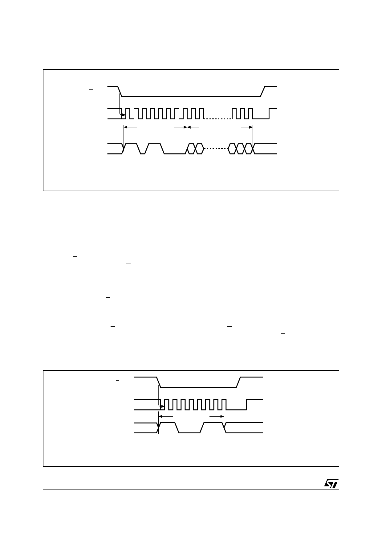
Figure 13. SE: Sector Erase Sequence
S
0123456789
29 30 31
C
INSTRUCTION
24 BIT ADDRESS
D
23 22
210
MSB
Note: 1. Address bits A23 to A17 are Don’t Care on the M25P10 series.
AI03751
the device once the Hardware Protected Mode is
entered.
The timing sequence is shown in Figure 10.
Sector Erase (SE)
Prior to any Sector Erase attempt, a write enable
instruction (WREN) must have been previously
sent (the S input driven low, WREN instruction
properly transmitted and the S input driven high).
After the WREN instruction decoding, the memory
sets the Write Enable Latch (WEL) which allows
the execution of any further Sector Erase. The
Sector Erase instruction is entered by driving the
Chip select input (S) low, followed by the
instruction byte and 3 address bytes on Data In
input (D). Any address of the Sector (see Table 4)
is a valid address for the Sector Erase instruction.
The Chip Select input (S) must be driven low for
the entire duration of the sequence. The device
must be deselected just after the eighth bit of the
last address byte has been latched in. If not, the
Sector Erase instruction is not executed. As soon
as the device is deselected, the self-timed Sector
Erase cycle (tSE) is initiated. While the Sector
Erase cycle is in progress, the status register may
be read to check the WIP bit value. WIP is high
during the self-timed Sector Erase cycle and is low
when it is completed. When the cycle is
completed, the write enable latch (WEL) is reset.
A Sector Erase instruction applied to a Sector
which is software protected by the BPi bits (see
Table 4 and Table 5) is not initiated.
The timing sequence is shown in Figure 13.
Bulk Erase (BE)
Prior to any Bulk Erase attempt, a write enable
instruction (WREN) must have been previously
sent (the S input driven low, WREN instruction
properly transmitted and the S input driven high).
After the WREN instruction decoding, the memory
Figure 14. BE: Bulk Erase Sequence
S
01234567
C
INSTRUCTION
D
10/21
AI03752
Share Link: 