FM25V01 Просмотр технического описания (PDF) - Cypress Semiconductor
Номер в каталоге
Компоненты Описание
Список матч
FM25V01 Datasheet PDF : 18 Pages
| |||
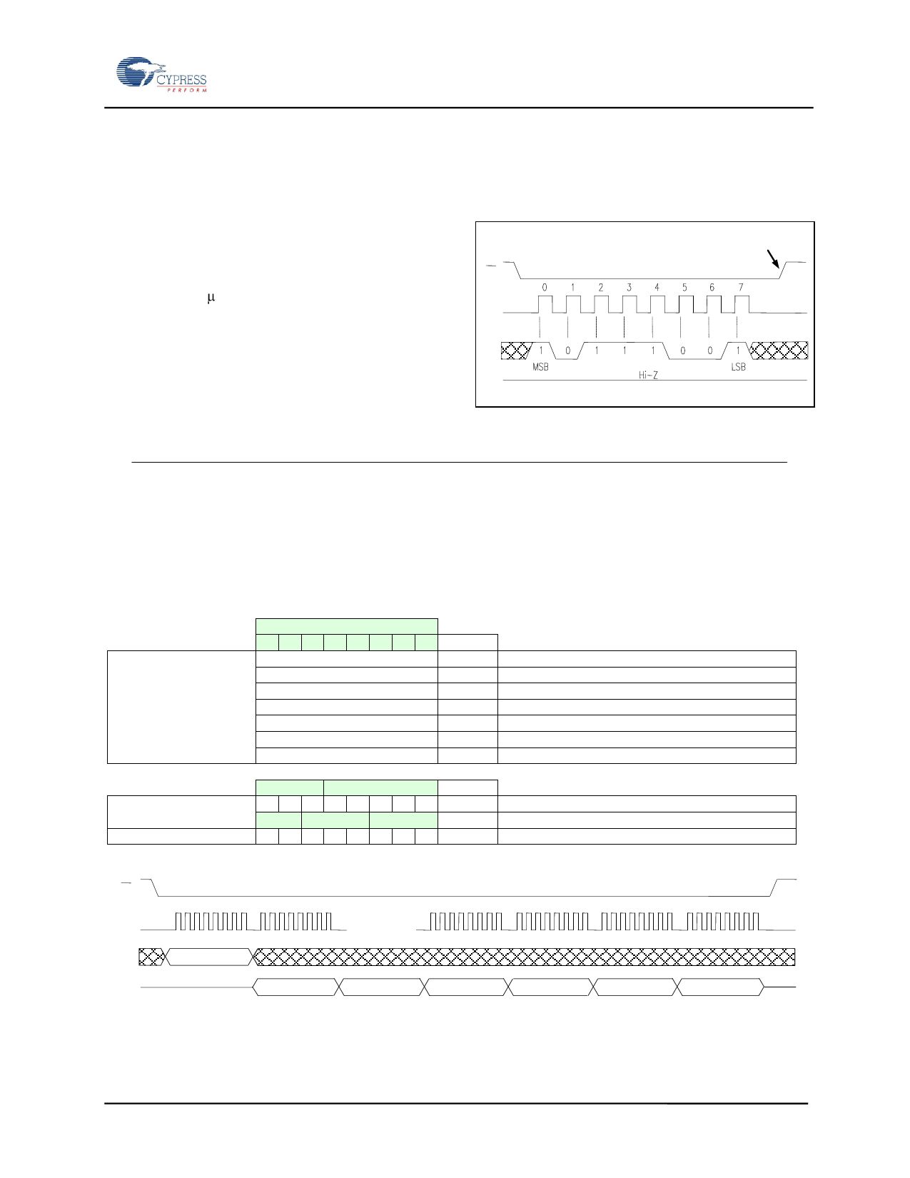
Sleep Mode
A low power mode called Sleep Mode is
implemented on the FM25V01 device. The device
will enter this low power state when the SLEEP op-
code B9h is clocked-in and a rising edge of /S is
applied. Once in sleep mode, the C and D pins are
ignored and Q will be high-Z, but the device
continues to monitor the /S pin. On the next falling
edge of /S, the device will return to normal operation
within tREC (400 s max.). The Q pin remains in a hi-
Z state during the wakeup period. The device will not
necessarily respond to an opcode within the wakeup
period. To start the wakeup procedure, the controller
may send a “dummy” read, for example, and wait the
remaining tREC time. It is not recommended to start
the wakeup by asserting /S low, leaving /S low, and
issuing clocks since the device wakeup is an
asynchronous event and could misinterpret the
FM25V01 - 128Kb SPI FRAM
opcodes. It is recommended that the controller
deassert /S after each polled read opcode. Polling is
the process of looking for expected data and allows
the system to determine if the device has returned to
a normal operating condition.
Enter Sleep
Mode
S
C
D
Q
Figure 12. Sleep Mode Entry
Device ID
The FM25V01 device can be interrogated for its manufacturer, product identification, and die revision. The RDID
op-code 9Fh allows the user to read the manufacturer ID and product ID, both of which are read-only bytes. The
JEDEC-assigned manufacturer ID places the Ramtron identifier in bank 7, therefore there are six bytes of the
continuation code 7Fh followed by the single byte C2h. There are two bytes of product ID, which includes a Family
code, a Density code, a Sub code, and Product Revision code.
Table 6. Manufacturer and Product ID
Manufacturer ID
Bit
7 6 5 4 3 2 1 0 Hex
0 1 1 1 1 1 1 1 7F Continuation code
0 1 1 1 1 1 1 1 7F Continuation code
0 1 1 1 1 1 1 1 7F Continuation code
0 1 1 1 1 1 1 1 7F Continuation code
0 1 1 1 1 1 1 1 7F Continuation code
0 1 1 1 1 1 1 1 7F Continuation code
1 1 0 0 0 0 1 0 C2 JEDEC assigned Ramtron C2h in bank 7
Device ID (1st Byte)
Device ID (2nd Byte)
Family
Density
Hex
0 0 1 0 0 0 0 1 21h Density: 01h=128K, 02h=256K, 03h=512K, 04=1M
Sub Rev.
Rsvd
0 0 0 0 0 0 0 0 00h 00h=FM25V01
S
C
.......
D
9Fh
Q
7Fh
…
7Fh
C2h
21h
00h
1
6
Six bytes of continuation code 7Fh
Figure 13. Read Device ID
Document Number: 001-84492 Rev. *B
Page 9 of 18
Share Link: 