FM25V01 Просмотр технического описания (PDF) - Cypress Semiconductor
Номер в каталоге
Компоненты Описание
Список матч
FM25V01 Datasheet PDF : 18 Pages
| |||
FM25V01 - 128Kb SPI FRAM
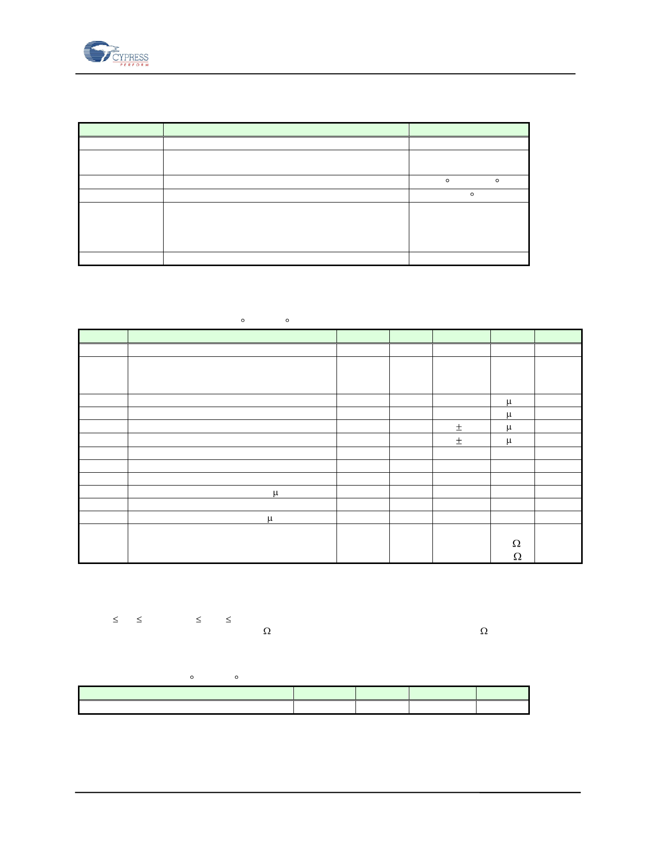
Electrical Specifications
Absolute Maximum Ratings
Symbol
Description
VDD
Power Supply Voltage with respect to VSS
VIN
Voltage on any pin with respect to VSS
TSTG
TLEAD
VESD
Storage Temperature
Lead Temperature (Soldering, 10 seconds)
Electrostatic Discharge Voltage
- Human Body Model (AEC-Q100-002 Rev. E)
- Charged Device Model (AEC-Q100-011 Rev. B)
- Machine Model (AEC-Q100-003 Rev. E)
Package Moisture Sensitivity Level
Ratings
-1.0V to +4.5V
-1.0V to +4.5V
and VIN < VDD+1.0V
-55 C to + 125 C
260 C
TBD
1.25kV
200V
MSL-1
Stresses above those listed under Absolute Maximum Ratings may cause permanent damage to the device. This is a stress rating
only, and the functional operation of the device at these or any other conditions above those listed in the operational section of this
specification is not implied. Exposure to absolute maximum ratings conditions for extended periods may affect device reliability.
DC Operating Conditions (TA = -40 C to + 85 C, VDD = 2.0V to 3.6V unless otherwise specified)
Symbol Parameter
Min
Typ
Max
Units Notes
VDD
Power Supply Voltage
IDD
Power Supply Operating Current
@ C = 1 MHz
2.0
3.3
3.6
V
1
0.12
0.22
mA
@ C = 40 MHz
1.3
2.5
mA
ISB
Standby Current
IZZ
Sleep Mode Current
ILI
Input Leakage Current
ILO
Output Leakage Current
90
150
A
2
5
8
A
3
-
1
A
4
-
1
A
4
VIH
VIL
VOH1
VOH2
VOL1
VOL2
RIN
Input High Voltage
Input Low Voltage
Output High Voltage (IOH = -1 mA, VDD=2.7V)
Output High Voltage (IOH = -100 A)
Output Low Voltage (IOL = 2 mA, VDD=2.7V)
Output Low Voltage (IOL = 150 A)
Input Resistance (/HOLD pin)
For VIN = VIH (min)
For VIN = VIL (max)
0.7 VDD
-0.3
2.4
VDD-0.2
-
-
40
1
VDD + 0.3
V
0.3 VDD
V
-
V
-
V
0.4
V
0.2
V
5
K
M
Notes
1. C toggling between VDD-0.2V and VSS, other inputs VSS or VDD-0.2V.
2. /S=VDD. All inputs VSS or VDD.
3. In Sleep mode and /S=VDD. All inputs VSS or VDD.
4. VSS VIN VDD and VSS VOUT VDD.
5. The input pull-up circuit is stronger (> 40K ) when the input voltage is above VIH and weak (> 1M ) when the input
voltage is below VIL.
Data Retention (TA = -40 C to + 85 C)
Parameter
Data Retention
Min
Max
Units
Notes
10
-
Years
Document Number: 001-84492 Rev. *B
Page 11 of 18
Share Link: 