FM25V01 Просмотр технического описания (PDF) - Cypress Semiconductor
Номер в каталоге
Компоненты Описание
Список матч
FM25V01 Datasheet PDF : 18 Pages
| |||
W
S
HOLD
C
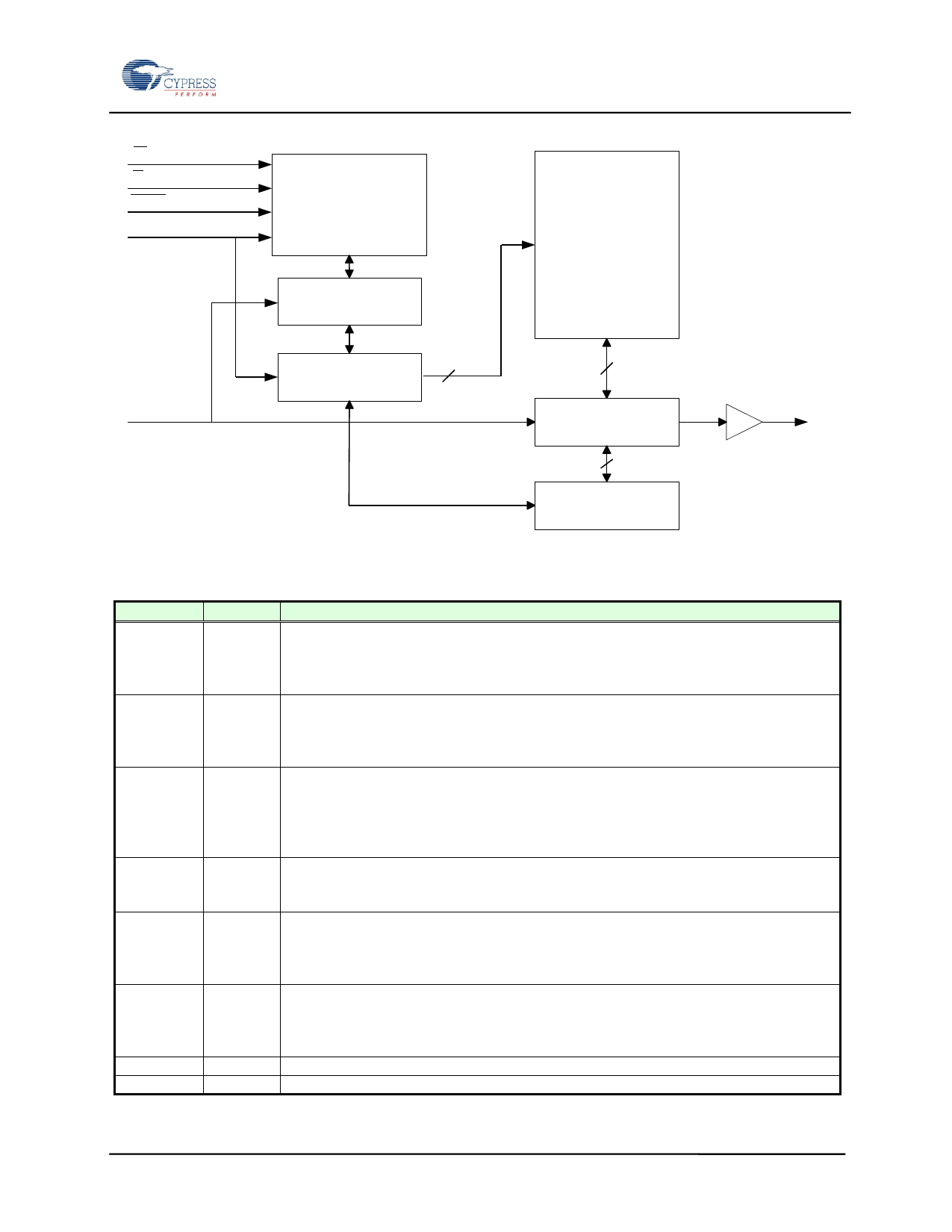
Instruction Decode
Clock Generator
Control Logic
Write Protect
Instruction Register
FM25V01 - 128Kb SPI FRAM
2K x 64
FRAM Array
Address Register
14
8
Counter
D
Q
Data I/O Register
3
Nonvolatile Status
Register
Pin Descriptions
Pin Name
/S
I/O
Input
C
Input
/HOLD
Input
/W
Input
D
Input
Q
Output
VDD
VSS
Supply
Supply
Figure 1. Block Diagram
Description
Chip Select: This active-low input activates the device. When high, the device enters
low-power standby mode, ignores other inputs, and all outputs are tri-stated. When
low, the device internally activates the C signal. A falling edge on /S must occur prior
to every op-code.
Serial Clock: All I/O activity is synchronized to the serial clock. Inputs are latched on
the rising edge and outputs occur on the falling edge. Since the device is static, the
clock frequency may be any value between 0 and 40 MHz and may be interrupted at
any time.
Hold: The /HOLD pin is used when the host CPU must interrupt a memory operation
for another task. When /HOLD is low, the current operation is suspended. The device
ignores any transition on C or /S. All transitions on /HOLD must occur while C is low.
This pin has a weak internal pull-up (see RIN spec, pg 11). However, if it is not used,
the /HOLD pin should be tied to VDD.
Write Protect: This active-low pin prevents write operations to the Status Register
only. A complete explanation of write protection is provided on pages 6 and 7. If not
used, the /W pin should be tied to VDD.
Serial Input: All data is input to the device on this pin. The pin is sampled on the
rising edge of C and is ignored at other times. It should always be driven to a valid
logic level to meet IDD specifications.
* D may be connected to Q for a single pin data interface.
Serial Output: This is the data output pin. It is driven during a read and remains tri-
stated at all other times including when /HOLD is low. Data transitions are driven on
the falling edge of the serial clock.
* Q may be connected to D for a single pin data interface.
Power Supply
Ground
Document Number: 001-84492 Rev. *B
Page 2 of 18
Share Link: 