FM25V01 Просмотр технического описания (PDF) - Cypress Semiconductor
Номер в каталоге
Компоненты Описание
Список матч
FM25V01 Datasheet PDF : 18 Pages
| |||
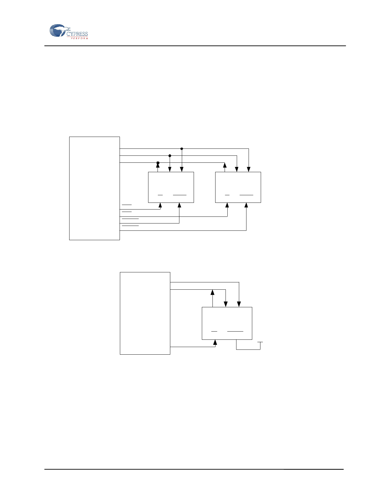
System Hookup
The SPI interface uses a total of four pins: clock,
data-in, data-out, and chip select. A typical system
configuration uses one or more FM25V01 devices
with a microcontroller that has a dedicated SPI port,
as Figure 3 illustrates. Note that the clock, data-in,
and data-out pins are common among all devices.
The Chip Select and Hold pins must be driven
separately for each FM25V01 device.
FM25V01 - 128Kb SPI FRAM
For a microcontroller that has no dedicated SPI bus, a
general purpose port may be used. To reduce
hardware resources on the controller, it is possible to
connect the two data pins together and tie off the
Hold pin. Figure 4 shows a configuration that uses
only three pins.
SCK
MOSI
MISO
SPI
Microcontroller
SS1
SS2
HOLD1
HOLD2
Q DC
FM25V01
S HOLD
QD C
FM25V01
S HOLD
MOSI : Master Out Slave In
MISO : Master In Slave Out
SS : Slave Select
Figure 3. 256Kbit (32KB) System Configuration with SPI port
P1.0
P1.1
Microcontroller
P1.2
QDC
FM25V01
S HOLD Vdd
Figure 4. System Configuration without SPI port
Document Number: 001-84492 Rev. *B
Page 4 of 18
Share Link: 