FM25V01 Просмотр технического описания (PDF) - Cypress Semiconductor
Номер в каталоге
Компоненты Описание
Список матч
FM25V01 Datasheet PDF : 18 Pages
| |||
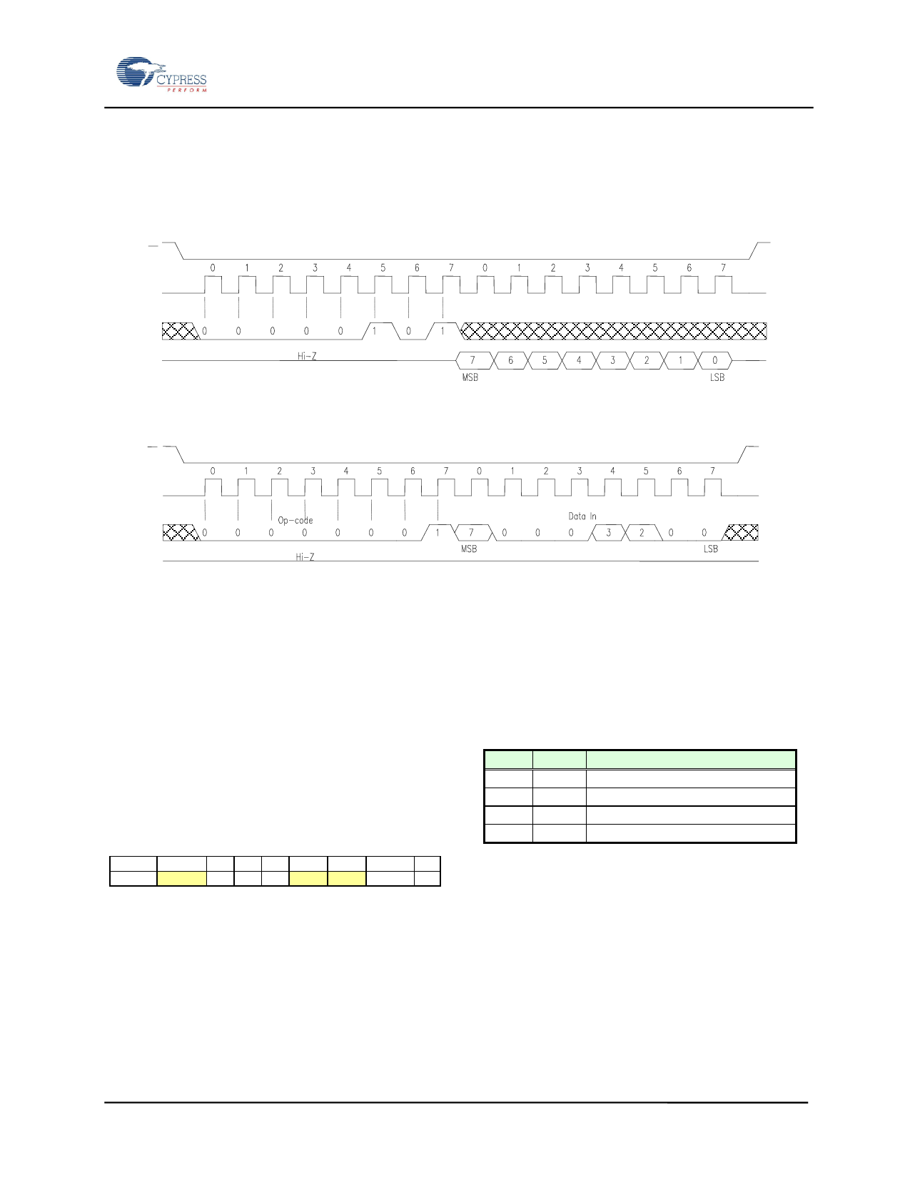
WRSR – Write Status Register
The WRSR command allows the user to select
certain write protection features by writing a byte to
the Status Register. Prior to issuing a WRSR
command, the /W pin must be high or inactive. Prior
S
C
FM25V01 - 128Kb SPI FRAM
to sending the WRSR command, the user must send
a WREN command to enable writes. Note that
executing a WRSR command is a write operation
and therefore clears the Write Enable Latch. The bus
configuration of RDSR and WRSR are shown
below.
D
Q
Figure 7. RDSR Timing
S
C
D
Q
Figure 8. WRSR Timing (WREN not shown)
Status Register & Write Protection
The write protection features of the FM25V01 are
multi-tiered. Taking the /W pin to a logic low state is
the hardware write-protect function. Status Register
write operations are blocked when /W is low. To
write the memory with /W high, a WREN op-code
must first be issued. Assuming that writes are enabled
using WREN and by /W, writes to memory are
controlled by the Status Register. As described
above, writes to the Status Register are performed
using the WRSR command and subject to the /W pin.
The Status Register is organized as follows.
Table 2. Status Register
Bit
7
654
3
2
1
0
Name WPEN 0 0 0 BP1 BP0 WEL 0
Bits 0 and 4-6 are fixed at 0, and cannot can be
modified. Note that bit 0 (“Ready” in Serial Flash) is
unnecessary as the F-RAM writes in real-time and is
never busy, so it reads out as a „0‟. There is an
exception to this when the device is waking up from
Sleep Mode, which is described on the following
page. The BP1 and BP0 control software write
protection features. They are nonvolatile (shaded
yellow). The WEL flag indicates the state of the
Write Enable Latch. Attempting to directly write the
WEL bit in the Status Register has no effect on its
Document Number: 001-84492 Rev. *B
state. This bit is internally set and cleared via the
WREN and WRDI commands, respectively.
BP1 and BP0 are memory block write protection bits.
They specify portions of memory that are write-
protected as shown in the following table.
Table 3. Block Memory Write Protection
BP1 BP0 Protected Address Range
0
0 None
0
1 3000h to 3FFFh (upper ¼)
1
0 2000h to 3FFFh (upper ½)
1
1 0000h to 3FFFh (all)
The BP1 and BP0 bits and the Write Enable Latch
are the only mechanisms that protect the memory
from writes. The remaining write protection features
protect inadvertent changes to the block protect bits.
The WPEN bit controls the effect of the hardware /W
pin. When WPEN is low, the /W pin is ignored.
When WPEN is high, the /W pin controls write
access to the Status Register. Thus the Status Register
is write protected if WPEN=1 and /W=0.
This scheme provides a write protection mechanism,
which can prevent software from writing the memory
under any circumstances. This occurs if the BP1 and
Page 6 of 18
Share Link: 