AN1042 Просмотр технического описания (PDF) - ON Semiconductor
Номер в каталоге
Компоненты Описание
Список матч
AN1042 Datasheet PDF : 12 Pages
| |||
AN1042/D
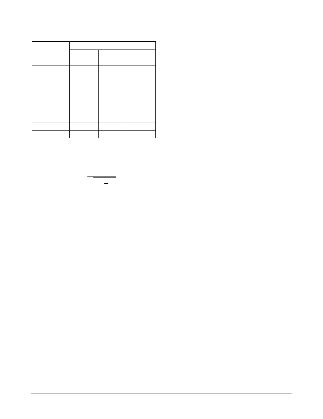
Table 2. Frequency Spectrum of Switching Amplifier
Carrier Frequency = 100 kHz with 20 kHz Sine Wave Modulation
Harmonic
Number
Percent of Rated Power
100%
50%
25%
Fundamental
0.988
0.498
0.25
2
0
0
0
3
0.183
0.053
0.014
4
0
0
0
5
0.600
1.084
1.224
6
0
0
0
7
0.506
0.147
0.036
8
0
0
0
9
0.366
0.391
0.235
10
0
0
0
With both the 80 and 100 kHz carriers, a 6 pole
Butterworth filter will be necessary in order to reduce the
residual carrier to acceptable levels. It has a much sharper
cutoff than a 4 pole filter and a transfer function of
Ǹ ǒ Ǔ Eout +
1
1)
f
fc
12
A cutoff frequency of 20 kHz will be assumed.
Note that the carrier increases as output level is reduced.
The carrier for 100%, 50% and 25% output is 0.600, 1.084,
and 1.224 respectively. The 80 kHz and 100 kHz carriers
will be attenuated by 72 and 84 dB respectively. The filter
in the amplifier described here attenuates its 120 kHz
carrier by 62 dB.
With an 80 kHz carrier a lower sideband will occur at
40 kHz and will have an amplitude of 18.6% of the
fundamental at full output. At half output, this sideband
will be reduced to 9.6% and further reduced to 4.8% at
one–fourth output. This sideband will appear as second
harmonic distortion of the fundamental. After the filter,
second harmonic levels will be 0.3%, 0.15%, and 0.075%
for full, half, and quarter output levels. At full output the
fundamental is only 98% of normal. Second harmonic
distortion does not occur with a 100 kHz carrier and 20 kHz
modulation.
The practical lower limit for the switching frequency
appears to be 4 times the maximum signal frequency. Even
if the difficulties associated with modulation are
overcome, operation at 3 times signal frequency will
require an 8 pole Butterworth filter. This will negate any
advantage in lower switching losses. At this low carrier
frequency, the first lower side band appears on top of the
output frequency. An undesirable beat between that
sideband and the output frequency results.
As the switching frequency is lowered, the error voltage
integrator in Figure 6 must be made more sluggish to keep
the ac component of the error voltage within common
mode range of the duty cycle comparator. This effectively
reduces the high frequency feedback and increases the
distortion in the vicinity of 5 kHz. It also slows the transient
response of the amplifier. More exotic means may be used
for filtering the error voltage, but many of these introduce
phase shift that makes the feedback loop unstable.
One of the more outstanding features of a switching
amplifier is that it has absolutely no crossover distortion.
This is true only so long as there are no operational
amplifiers or analog transistors in the signal path that have
such distortion. In the amplifier described here, the
MC14573/575 series of operational amplifiers have class
A output stages that meet this criterion. Digital circuitry
passing the variable duty cycle waveform cannot introduce
crossover distortion.
Conventional amplifiers overheat readily when operated
into highly reactive loads. The power wasted in a class B
amplifier
with
a
reactive
load
is
4
4*
p
+
4.66
times
the
power wasted with a resistive load. A 600 Hz test was done
using a 2 millihenry choke for a load. A 1000 Hz test was
also done using a 20 microfarad polypropylene capacitor as
a load. Both have a reactance of 8 ohms at the test
frequency. The only results of note were slight heating of
the choke and lack of any appreciable power taken from the
line. Heatsink temperatures were the same as when a
resistive load was used. A conventional amplifier with
normal sized heatsinks would have burned up under those
conditions. If reactive loads are driven, resonances must be
avoided in the output filter.
During the later stages of development, the author
received a complaint about an audible high frequency
whine coming from the amplifier. A few tenths of a volt of
10 kHz sinewave were found on the outputs of both
channels. This 10 kHz signal was locked to the power
supply 20 kHz. No flip flops existed that were capable of
dividing the power supply frequency by two. Shorting the
input of the amplifier did not help. An audio spectrum
analyzer finally found a few millivolts of 10 kHz signal
riding on the 120 kHz triangle.
An MC14046 Phase Locked Loop had been used to lock
the switching frequency to the power supply frequency.
Hunting in the loop was producing the 10 kHz. This caused
a small amount of am and fm on the 120 kHz triangle. This
PLL has about 0.1 microsecond of time crossover
distortion in the vicinity of phase lock. The distortion
comes from internal lead lag flip flop switching near lock.
Introducing a few tenths of a microsecond dc offset with a
bias resistor cured the problem. Great care must be taken
to achieve a stable loop. If a PLL is not used, the power
supply should be driven at a frequency synchronous with
the switching frequency to avoid troublesome beats and
distortion products.
A complete discussion of RFI elimination is also beyond
the scope of this paper. The author operated the left and
right channels of the amplifier out of phase at their
http://onsemi.com
9
Share Link: 