AN1042 Просмотр технического описания (PDF) - ON Semiconductor
Номер в каталоге
Компоненты Описание
Список матч
AN1042 Datasheet PDF : 12 Pages
| |||
AN1042/D
5
4
3
Parallel
2
Resonance
1
11.4 kHz
Parallel
0
Series
Resonance
–1
Resonance
35.2 kHz
20 kHz
–2
–3
–4
–5
0
12
24
36
48
60
kHz
Figure 4. Four Pole Butterworth Filter
Output Impedance
The amplifier output impedance at dc is about 4
milliohms and gradually becomes inductive. At 100 Hz, its
output impedance is 0.1 ohm giving a damping factor of 80.
Damping factor is the ratio of load impedance to amplifier
output impedance.
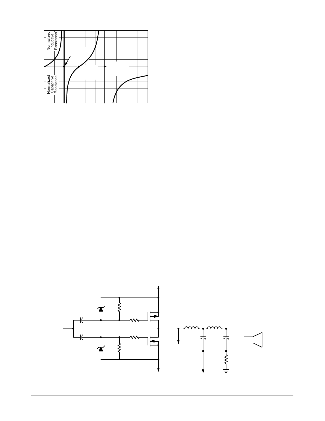
The complementary power MOSFET output stage of the
amplifier is shown in Figure 5. It generates a ±44 volt
square wave whose duty cycle can vary from 5% to 95%.
This variable duty cycle square wave is fed to the output
filter where the low frequency component is passed on to
the 8 ohm speaker. This filter allows frequencies under
20 kHz to pass with negligible loss, but greatly attenuates
the switching frequency. Since both sources are connected
to a supply rail, a drive of 10 volts peak to peak on each gate
insures full turn on. A buffer amp using ±5 volts supplies
provides this drive.
The 4.7 ohm resistors, R17 and R18, in each gate lead
prevents high frequency oscillation during switching. The 12
volt Zeners, CR3 and CR4, serve both as conventional
diode clamps and provide static discharge protection. They
act as dc restorers, and are made necessary by the ac
coupling. The 10 k resistors, R15 and R16, provide a slight
discharge path to keep conduction pulses in the clamp
diodes. They also discharge the gates in about 1
millisecond if the drive signal is lost. About 9 volts of
turn–on bias is applied to each gate. Tight coupling
between the gates prevents simultaneous turn–on of both
devices.
The output stage inverts the drive signal and generates
rise and fall times of about 30 nanoseconds. It is designed
to put out a maximum current of ±5 amps down to a
frequency of 0.1 Hertz. Below that frequency, maximum
current may need to be derated to prevent alternate
overheating of each output device. Excessive heatsink
temperature increases the ON resistance and the storage
time of the source drain diode. The resultant increase in
losses can lead to thermal runaway.
The drive waveform duty cycle must be a linear function
of the control voltage. The Duty Cycle Controller is shown
in Figure 6. A square wave of ±5 volts at 120 kHz is coupled
through C1 and R1 to integrator U1B. C1 blocks dc and R1
is the integrator resistor. C2 is the integrator capacitor
which generates a ±2 volt triangle on the output of U1B. R2
provides a small amount of dc leakage to insure that the
output has no significant dc component. R3 couples the
triangle to the noninverting input of comparator U1D. It
improves the waveform by isolating the input capacitance
of the comparator from the integrator. The dc offset on the
triangle is equal to the offset of U1B and its linearity is
better than 1%.
Input audio is applied to the inverting input of U2C
through R4. The output square wave of the power amp is
applied through R5 to the same summing point. U2C
functions as an integrator with C3 as the integrator
capacitor. Since R5 is 20 times R4, an inverting voltage
gain of 20 must result if the input of U2C is to be at ground.
The output of U2C serves as the error voltage and is fed to
the inverting input of U1D through R6 and R7. C4
eliminates short spikes on the error buss. Current limiting
circuitry is connected to the junction of R6 and R7. When
current drawn from the amplifier tries to exceed safe limits,
the error voltage is overridden and overcurrent is prevented.
+44
Drive
CR3 R15
C7
R17
C8
CR4
R18
R16
Q3
L1
L2
Q4
Feedback
C9
C10
R27
Current Sense
Figure 5. Output Circuit of a Class D Amplifier
http://onsemi.com
3
8Ω
Speaker
Share Link: 