AN1042 Просмотр технического описания (PDF) - ON Semiconductor
Номер в каталоге
Компоненты Описание
Список матч
AN1042 Datasheet PDF : 12 Pages
| |||
AN1042/D
+5
120 kHz
–5
R1
C1
C2
R2
U1B
+2
R3 –2
+
U1D
–
(Comparator)
Variable
Duty Cycle
Output
Audio
R4
Input
R8
C3
R6
R7
U2C
C4
Current
Compensation
R5
From Output
From Current
Limit
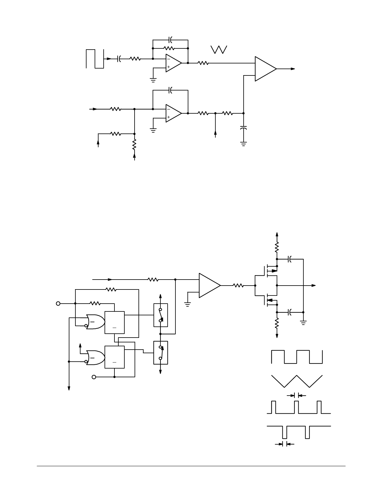
Figure 6. Duty Cycle Controller
The ±2 volt triangle is applied to the non–inverting input
of U1D. The error voltage normally varies over this same
range. As it does so, the output of U1D is a square wave at
120 kHz whose duty cycle varies from 0% to 100%. The
error voltage will exceed normal limits if the amplifier
should clip. In that case, the output drive waveform will
lock up at either +5 or –5 volts. If not corrected, the ac
coupling of the drive signal would cause a loss of drive to
the final amplifiers and associated severe distortion.
To prevent loss of drive, the drive waveform duty cycle
must be restricted to the range of 5% to 95%. This is
accomplished by the circuit of Figure 7. The 120 kHz square
R13
C5
+5 V
Variable
Duty
Cycle
R11 R10
A
B
–5 V
A
B
Q
U3A
R
Q
U3B
R
R9
+5 V
U4A
U4B
–
R12
U1C
+
(Comparator)
Q1
Q2
C6
R14
–5
120 kHz
Input –5 V
Drive to
Switches
+5 V
120 kHz
–5 V
Integrator
Output
U1B
+2 V
–2 V
Variable
Duty Cycle
U1D Output
+5 V
High Limit
5%
–5 V
250 ns
+5 V
Low Limit
95% –5 V
250 ns
Figure 7. Schematic of Duty Cycle Limiter and Output Driver
http://onsemi.com
4
Share Link: 