AN1042 Просмотр технического описания (PDF) - ON Semiconductor
Номер в каталоге
Компоненты Описание
Список матч
AN1042 Datasheet PDF : 12 Pages
| |||
AN1042/D
wave clock is fed to a pair of CMOS monostables each of
which produces a 250 nanosecond pulse. Only timing
resistors are used and internal parasitics serve as the timing
capacitance. One monostable produces a pulse on the
positive transition of the square wave, and the other
produces a pulse on the negative transition. These short
pulses are connected to the control inputs of two CMOS
analog switches. When the 120 kHz square wave goes
positive, the upper CMOS switch turns on and the common
terminal is switches to + 5 volts. When the 120 kHz square
wave goes negative, the bottom CMOS switch turns on and
the common terminal is switched to –5 volts.
Since the drive signal from U1D is fed through R9, it will
be overridden if either of the CMOS switches is on. If the
error voltage to U1D is out of limits, its output will be
locked up at either +5 or –5 volts. The CMOS switches will
then act to insure either short negative or positive pulses to
the input of U1C. U1C is a comparator used as an inverting
buffer between the CMOS switches and the small signal
TMOS drivers. These devices have low input capacitance
and low output impedance.
The drive signal is fed through R12 to the gates of Q1 and
Q2. They function as a low impedance inverting buffer to
drive the output stage. Decoupling networks isolate the
sources of Q1 and Q2 from the ±5 volt supplies. This
prevents the disruption of other circuitry by the large
current spikes needed to drive the output stages. Note that
the feedback path from R5 to the output experiences 5
polarity inversions. They are U2C, U1D, U1C, Q1–Q2 and
Q3–Q4. An odd number of inversions is required to make
the overall feedback negative.
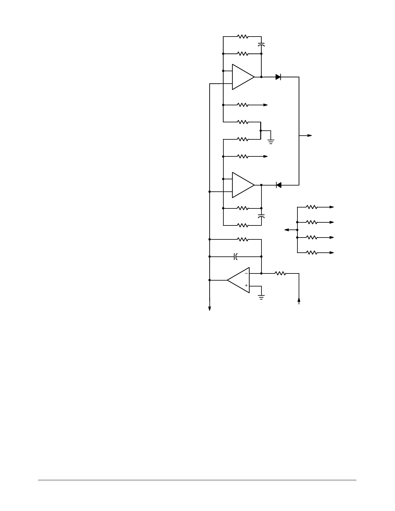
The current limiting circuitry is shown in Figure 8. R27,
a 0.05 ohm noninductive resistor, senses the ground current
in the output filter and speaker. The voltage across this
resistor is amplifier by op amp U2D. R28 and R29 set the
gain of U2D at 10. C11 rolls off the response above 300 kHz.
The level at the output of U2D is –0.5 volt per amp of output
current. The output of U2D is applied through R8 to the
error amp for filter resistance compensation as shown in
Figure 6. For every amp drawn by the speaker, the output
voltage is increased by about 0.1 volt. This compensates for
the loss in the filter and current sensing resistor. The
lowered output impedance at low frequencies improves
speaker damping.
The amplified current signal at the output of U2D is also
routed to the noninverting inputs of U2A and U2B. These
op amps are the current limiters. U2A limits negative
current and U2B limits positive current. Only U2A will be
described since U2B operates in an identical manner. R19
and R21 form a voltage divider with an output of 2.5 volts.
This voltage is applied to the inverting input of U2A. When
the non–inverting input of U2A is more positive than 2.5
volts, the speaker current is greater than –5 amps. In that
case, the output of U2A will rise towards +5 volts. This
output coupled through CR1 takes over control of the error
voltage buss. A voltage between ±2 volts is rapidly reached
R25
C12
R23
–
U2A
+
(Op Amp)
CR1
+5
R21
R19
R20
–5
R22
(Op Amp)
–
U2B
+
CR2
R24
R26
C13
–5 V
R29
C11
R28
U2D
(Op Amp)
Current
Limit
R30
U1 Pin 8
R31
U1 Pin 9
R32
U2 Pin 8
R33
U2 Pin 9
Current
Compensation
From Current
Sense Resistor
Figure 8. Schematic of Current Limiting and
Current Sense Amplifier
at the output of CR1 to limit the current at –5 amps. Note
that U2B has +5 volts for its output at this time and CR2 is
reverse biased. R23 limits the low frequency gain of U2A
to 45. R25 in conjunction with C12 limits the high
frequency gain. If the output current exceeds –5 amps by
as little as 0.1 amp, the output voltage can be reduced to
zero from full voltage.
The resistor–capacitor combination of R25 and C12
form a lag compensation filter. They are necessary because
the output inductors introduce a 90° lag in output current
near 1 kHz when the output is shorted. The values chosen
for the lag filter are a compromise between speed of
response and stability under short circuit conditions. An
overcurrent of 0.1 amp requires about 50 microseconds to
http://onsemi.com
5
Share Link: 