ADM4850 Просмотр технического описания (PDF) - Analog Devices
Номер в каталоге
Компоненты Описание
Список матч
ADM4850 Datasheet PDF : 16 Pages
| |||
ADM4850/ADM4851/ADM4852/ADM4853/ADM4854/ADM4855/ADM4856/ADM4857
PIN CONFIGURATIONS AND FUNCTION DESCRIPTIONS
ADM4850/ADM4851/
ADM4852/ADM4853
RO 1 ADM4850/ 8 VCC
ADM4851/
RE 2 ADM4852/ 7 B
DE 3 ADM4853 6 A
TOP VIEW
DI 4 (Not to Scale) 5 GND
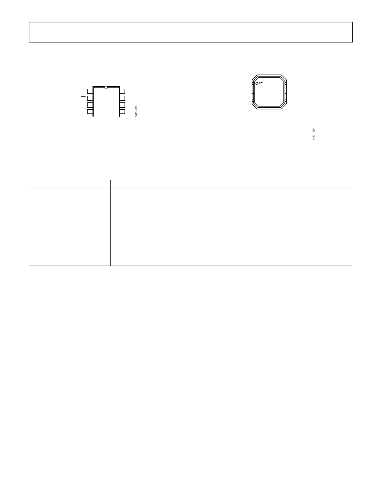
Figure 3. ADM4850/ADM4851/ADM4852/ADM4853 Pin Configuration,
SOIC and MSOP
RO 1
RE 2
DE 3
DI 4
PIN 1
INDICATOR
TOP VIEW
(Not to Scale)
8 VCC
7B
6A
5 GND
NOTES
1. THE EXPOSED PADDLE ON THE UNDERSIDE
OF THE PACKAGE SHOULD BE SOLDERED
TO THE GROUND PLANE TO INCREASE THE
RELIABILITY OF THE SOLDER JOINTS AND
TO MAXIMIZE THE THERMAL CAPABILITY OF
THE PACKAGE.
Figure 4. ADM4850/ADM4851/ADM4852/ADM4853 Pin Configuration, LFCSP
Table 8. ADM4850/ADM4851/ADM4852/ADM4853 Pin Descriptions
Pin No.
Mnemonic
Description
1
RO
Receiver Output. When RO is enabled, if (A − B) ≥ −30 mV, RO = high; if (A − B) ≤ −200 mV, RO = low.
2
RE
Receiver Output Enable. A low level on this pin enables the receiver output, RO. A high level places RO
into a high impedance state.
3
DE
Driver Output Enable. A high level on this pin enables the driver differential outputs, A and B. A low level
places them into a high impedance state.
4
DI
Driver Input. When the driver is enabled, a logic low on DI forces A low and B high, whereas a logic high
on DI forces A high and B low.
5
GND
Ground.
6
A
Noninverting Receiver Input A/Noninverting Driver Output A.
7
B
Inverting Receiver Input B/Inverting Driver Output B.
8
VCC
5 V Power Supply.
Rev. D | Page 7 of 16
Share Link: 