ADM4850 Просмотр технического описания (PDF) - Analog Devices
Номер в каталоге
Компоненты Описание
Список матч
ADM4850 Datasheet PDF : 16 Pages
| |||
ADM4850/ADM4851/ADM4852/ADM4853/ADM4854/ADM4855/ADM4856/ADM4857
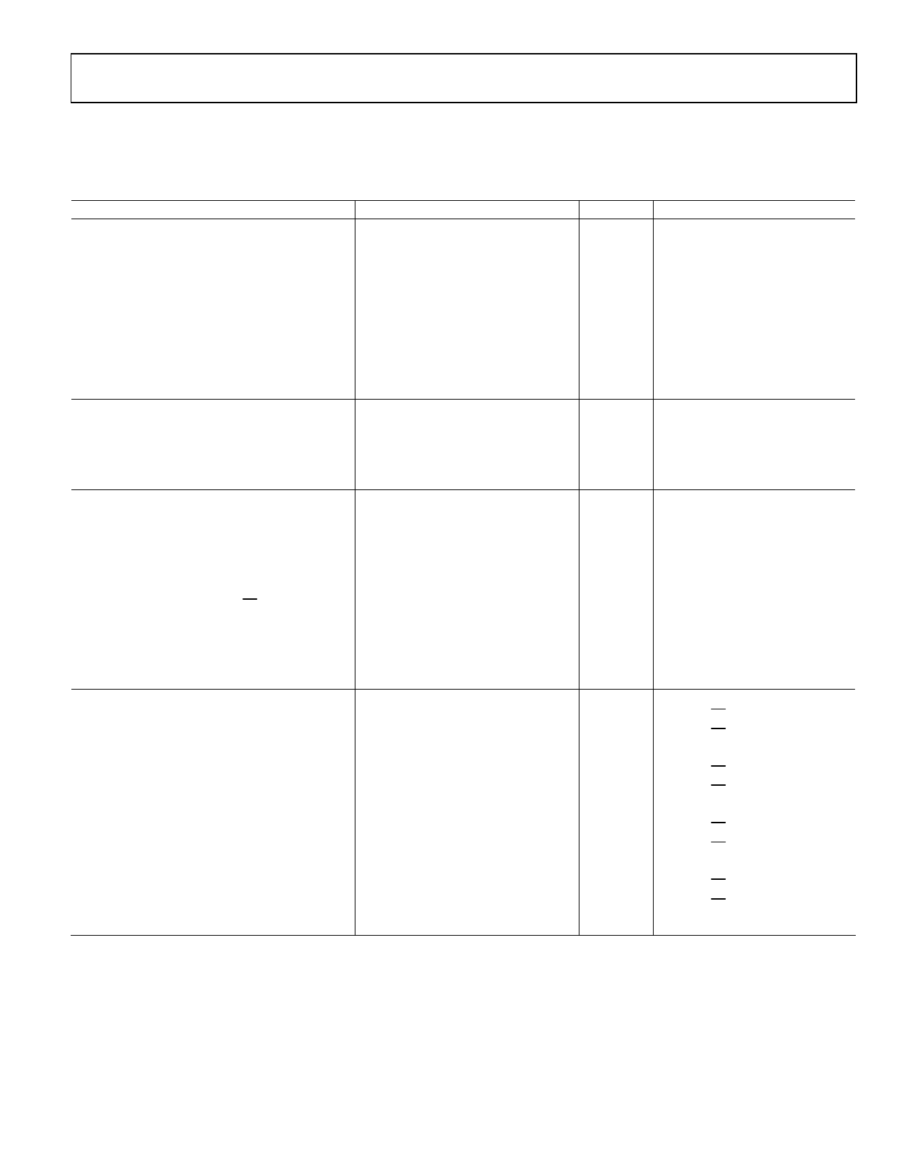
SPECIFICATIONS
VCC = 5 V ± 5%, TA = TMIN to TMAX, unless otherwise noted.
Table 2.
Parameter
Min
Typ
Max
Unit
DRIVER
Differential Output Voltage, VOD
2.0
VCC
V
5
V
1.5
5
V
|VOD3|
1.5
5
V
∆|VOD| for Complementary Output States
0.2
V
Common-Mode Output Voltage, VOC
∆|VOC| for Complementary Output States
Output Short-Circuit Current, VOUT = High
Output Short-Circuit Current, VOUT = Low
−200
−200
3
V
0.2
V
+200
mA
+200
mA
DRIVER INPUT LOGIC
CMOS Input Logic Threshold Low
0.8
V
CMOS Input Logic Threshold High
2.0
V
CMOS Logic Input Current (DI)
±1
μA
DE Input Resistance to GND
220
kΩ
RECEIVER
Differential Input Threshold Voltage, VTH
−200
−125
−30
mV
Input Hysteresis
20
mV
Input Resistance (A, B)
96
150
kΩ
Input Current (A, B)
0.125
mA
−0.1
mA
CMOS Logic Input Current (RE)
±1
μA
CMOS Output Voltage Low
0.4
V
CMOS Output Voltage High
4.0
V
Output Short-Circuit Current
7
85
mA
Three-State Output Leakage Current
±2
μA
POWER SUPPLY CURRENT
115 kbps Options (ADM4850/ADM4854)
5
μA
36
60
μA
100
160
μA
500 kbps Options (ADM4851/ADM4855)
5
μA
80
120
μA
120
200
μA
2.5 Mbps Options (ADM4852/ADM4856)
5
μA
250
400
μA
320
500
μA
10 Mbps Options (ADM4853/ADM4857)
5
μA
250
400
μA
320
500
μA
1 Guaranteed by design.
Test Conditions/Comments
R = ∞, see Figure 181
R = 50 Ω (RS-422), see Figure 18
R = 27 Ω (RS-485), see Figure 18
VTST = −7 V to 12 V, see Figure 19
R = 27 Ω or 50 Ω, see Figure 18
R = 27 Ω or 50 Ω, see Figure 18
R = 27 Ω or 50 Ω, see Figure 18
−7 V < VOUT < +12 V
−7 V < VOUT < +12 V
−7 V < VOC < +12 V
−7 V < VOC < +12 V
−7 V < VOC < +12 V
VIN = +12 V
VIN = −7 V
IOUT = +4 mA
IOUT = −4 mA
VOUT = GND or VCC
0.4 V ≤ VOUT ≤ 2.4 V
DE = 0 V, RE = VCC (shutdown)
DE = 0 V, RE = 0 V
DE = VCC
DE = 0 V, RE = VCC (shutdown)
DE = 0 V, RE = 0 V
DE = VCC
DE = 0 V, RE = VCC (shutdown)
DE = 0 V, RE = 0 V
DE = VCC
DE = 0 V, RE = VCC (shutdown)
DE = 0 V, RE = 0 V
DE = VCC
Rev. D | Page 3 of 16
Share Link: 