ADM4850 Просмотр технического описания (PDF) - Analog Devices
Номер в каталоге
Компоненты Описание
Список матч
ADM4850 Datasheet PDF : 16 Pages
| |||
5 V, Slew-Rate Limited, Half-Duplex and
Full-Duplex RS-485/RS-422 Transceivers
ADM4850/ADM4851/ADM4852/ADM4853/ADM4854/ADM4855/ADM4856/ADM4857
FEATURES
EIA RS-485-/RS-422-compliant
Data rate options
ADM4850/ADM4854: 115 kbps
ADM4851/ADM4855: 500 kbps
ADM4852/ADM4856: 2.5 Mbps
ADM4853/ADM4857: 10 Mbps
Half- and full-duplex options
Reduced slew rates for low EMI
True fail-safe receiver inputs
5 μA (maximum) supply current in shutdown mode
Up to 256 transceivers on one bus
Outputs high-Z when disabled or powered off
−7 V to +12 V bus common-mode range
Thermal shutdown and short-circuit protection
Pin-compatible with the MAX308x
Specified over the −40°C to +85°C temperature range
Available in 8-lead SOIC, LFCSP, and MSOP packages
Qualified for automotive applications
APPLICATIONS
Low power RS-485 applications
EMI-sensitive systems
DTE-DCE interfaces
Industrial control
Packet switching
Local area networks
Level translators
GENERAL DESCRIPTION
The ADM4850/ADM4851/ADM4852/ADM4853/ADM4854/
ADM4855/ADM4856/ADM4857 are differential line transceivers
suitable for high speed half- and full-duplex data communication on
multipoint bus transmission lines. They are designed for balanced
data transmission and comply with EIA Standards RS-485 and
RS-422. The ADM4850/ADM4851/ADM4852/ADM4853 are half-
duplex transceivers that share differential lines and have separate
enable inputs for the driver and receiver. The full-duplex
ADM4854/ADM4855/ADM4856/ADM4857 transceivers have
dedicated differential line driver outputs and receiver inputs.
The parts have a 1/8-unit-load receiver input impedance, which
allows up to 256 transceivers on one bus. Because only one driver
should be enabled at any time, the output of a disabled or pow-
ered-down driver is three-stated to avoid overloading the bus.
The receiver inputs have a true fail-safe feature, which ensures
a logic high output level when the inputs are open or shorted.
This guarantees that the receiver outputs are in a known state
Rev. D
Information furnished by Analog Devices is believed to be accurate and reliable. However, no
responsibility is assumed by Analog Devices for its use, nor for any infringements of patents or other
rights of third parties that may result from its use. Specifications subject to change without notice. No
license is granted by implication or otherwise under any patent or patent rights of Analog Devices.
Trademarks and registered trademarks are the property of their respective owners.
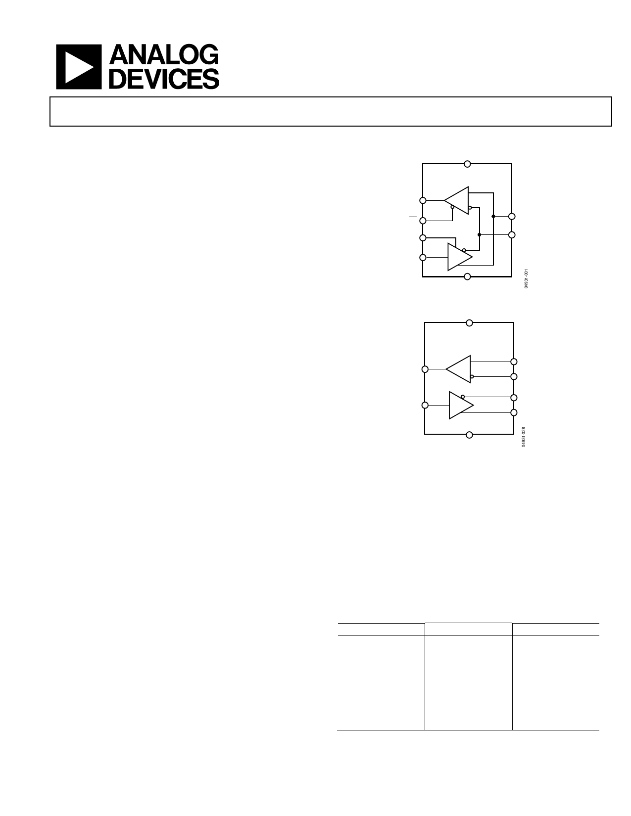
FUNCTIONAL BLOCK DIAGRAMS
VCC
ADM4850/ADM4851/
ADM4852/ADM4853
RO
R
A
RE
DE
B
DI
D
GND
Figure 1.
VCC
ADM4854/ADM4855/
ADM4856/ADM4857
A
RO
R
B
Z
DI
D
Y
GND
Figure 2.
before communication begins and when communication ends.
The driver outputs are slew-rate limited to reduce EMI and data
errors caused by reflections from improperly terminated buses.
Excessive power dissipation caused by bus contention or by output
shorting is prevented with a thermal shutdown circuit.
The parts are fully specified over the commercial and industrial
temperature ranges and are available in 8-lead SOIC, LFCSP
(ADM4850/ADM4851/ADM4852/ADM4853), and MSOP
(ADM4850 only) packages.
Table 1. Selection Table
Part No.
Half-/Full-Duplex
ADM4850
Half
ADM4851
Half
ADM4852
Half
ADM4853
Half
ADM4854
Full
ADM4855
Full
ADM4856
Full
ADM4857
Full
Data Rate
115 kbps
500 kbps
2.5 Mbps
10 Mbps
115 kbps
500 kbps
2.5 Mbps
10 Mbps
One Technology Way, P.O. Box 9106, Norwood, MA 02062-9106, U.S.A.
Tel: 781.329.4700
www.analog.com
Fax: 781.461.3113 ©2004–2012 Analog Devices, Inc. All rights reserved.
Share Link: 