GD25Q20 Просмотр технического описания (PDF) - Unspecified
Номер в каталоге
Компоненты Описание
Список матч
GD25Q20 Datasheet PDF : 38 Pages
| |||
The Write In Progress (WIP) bit indicates whether the memory is busy in program/erase/write status register progress.
When WIP bit sets to 1, means the device is busy in program/erase/write status register progress, when WIP bit sets 0,
means the device is not in program/erase/write status register progress.
WEL bit.
GD25Q20BxIGx The Write Enable Latch (WEL) bit indicUatensitfhoe rstmatussoef cthetoinrterdnaul Walritae nEndablqe uLaatcdh. Wseherniaselt tfola1 sthhe internal
Write Enable Latch is set, when set to 0 the internal Write Enable Latch is reset and no Write Status Register, Program or
Erase command is accepted.
BP4, BP3, BP2, BP1, BP0 bits.
The Block Protect (BP4, BP3, BP2, BP1, BP0) bits are non-volatile. They define the size of the area to be software
protected against Program and Erase commands. These bits are written with the Write Status Register (WRSR) command.
When the Block Protect (BP4, BP3, BP2, BP1, BP0) bits are set to 1, the relevant memory area (as defined in
Table1).becomes protected against Page Program (PP), Sector Erase (SE) and Block Erase (BE) commands. The Block
Protect (BP4, BP3, BP2, BP1, BP0) bits can be written provided that the Hardware Protected mode has not been set. The
Chip Erase (CE) command is executed, if the Block Protect (BP4,BP3,BP2, BP1, BP0) bits are set to “None protected”.
SRP0 bit.
The Status Register Protect (SRP0) bit is non-volatile Read/Write bits in the status register. The SRP bit controls the
method of write protection: software protection and hardware protection.
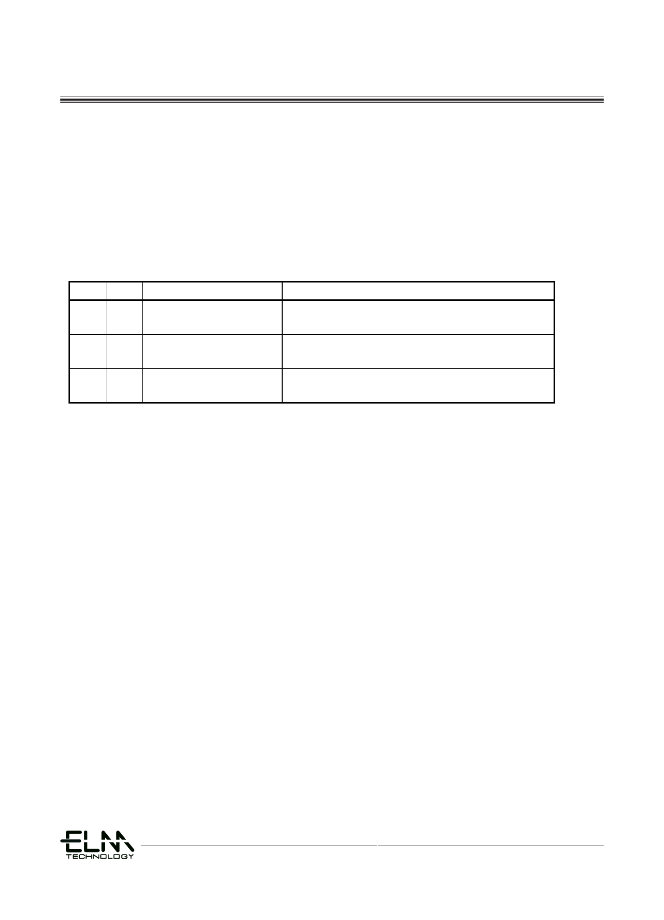
SRP0 #WP
Status Register
Description
0
X
Software Protected
The Status Register can be written to after a Write Enable
command, WEL=1.(Default)
1
0
Hardware Protected
WP#=0, the Status Register locked and can not be written to.
1
1
Hardware Unprotected
WP#=1, the Status Register is unlocked and can be written to
after a Write Enable command, WEL=1.
QE bit.
The Quad Enable (QE) bit is a non-volatile Read/Write bit in the Status Register that allows Quad operation. When
the QE bit is set to 0 (Default) the WP# pin and HOLD# pin are enable. When the QE bit is set to 1, the Quad IO2 and IO3
pins are enabled. (The QE bit should never be set to 1 during standard SPI or Dual SPI operation if the WP# or HOLD#
pins are tied directlyUtontihfeopromwer Ssueppclytoorrground)
CMP bit
UDnuiafol ramndSQecutaodr Serial Flash
GD25Q40B/20B
providTehemCorMePflebxitibiDsiliatuynafoonlr-tvahoenlaatdirleraQRyepuardoa/tWedcrtiitSoeneb. itPriilneaathlseeFSslteaaetustshheReSgtaisttuesr (rSeg1i4s)t.eIrtsisMuesmedoriyn PcorontjeuGcntcioDtinon2tat5hbelQeBf4oPr04d-BBePta/02ilsb0.itTsBhtoe
pdreofvaiudlet smeottrinegfliesxCibMiliPty=f0o.r the array protection. Please see the Status registers Memory Protection table for details. The
default setting is CMP=0.
SUS bit
SUS bTithe SUS bit are read only bit in the status register (S1514) that are set to 1 after executing an Erase/Program Suspend
(75H)TchoemSmUaSnbdi.t aTrheereSaUdSonbliyt bairteincltehaersetdattuos 0rebgyistEera(sSe1/P5 r)otghraatmarRe esseut mtoe1(a7fAteHr)ecxoemcumtinagndanasErwaseell/ParsogarapmowSeur-sdpoewnnd,
(p7o5wHe)rc-uopmcmyaclned.. The SUS bit are cleared to 0 by Erase/Program Resume (7AH) command as well as a power-down,
power-up cycle.
38 - 11
Rev.1.1
Share Link: 