W199 Просмотр технического описания (PDF) - Cypress Semiconductor
Номер в каталоге
Компоненты Описание
Список матч
W199 Datasheet PDF : 14 Pages
| |||
PRELIMINARY
W199
Writing Data Bytes
Each bit in Data Bytes 0–7 control a particular device function
except for the “reserved” bits which must be written as a logic
0. Bits are written MSB (most significant bit) first, which is bit 7.
Table 5 gives the bit formats for registers located in Data Bytes
0–7.
Table 6 details additional frequency selections that are avail-
able through the serial data interface.
Table 7 details the select functions for Byte 0, bits 1 and 0.
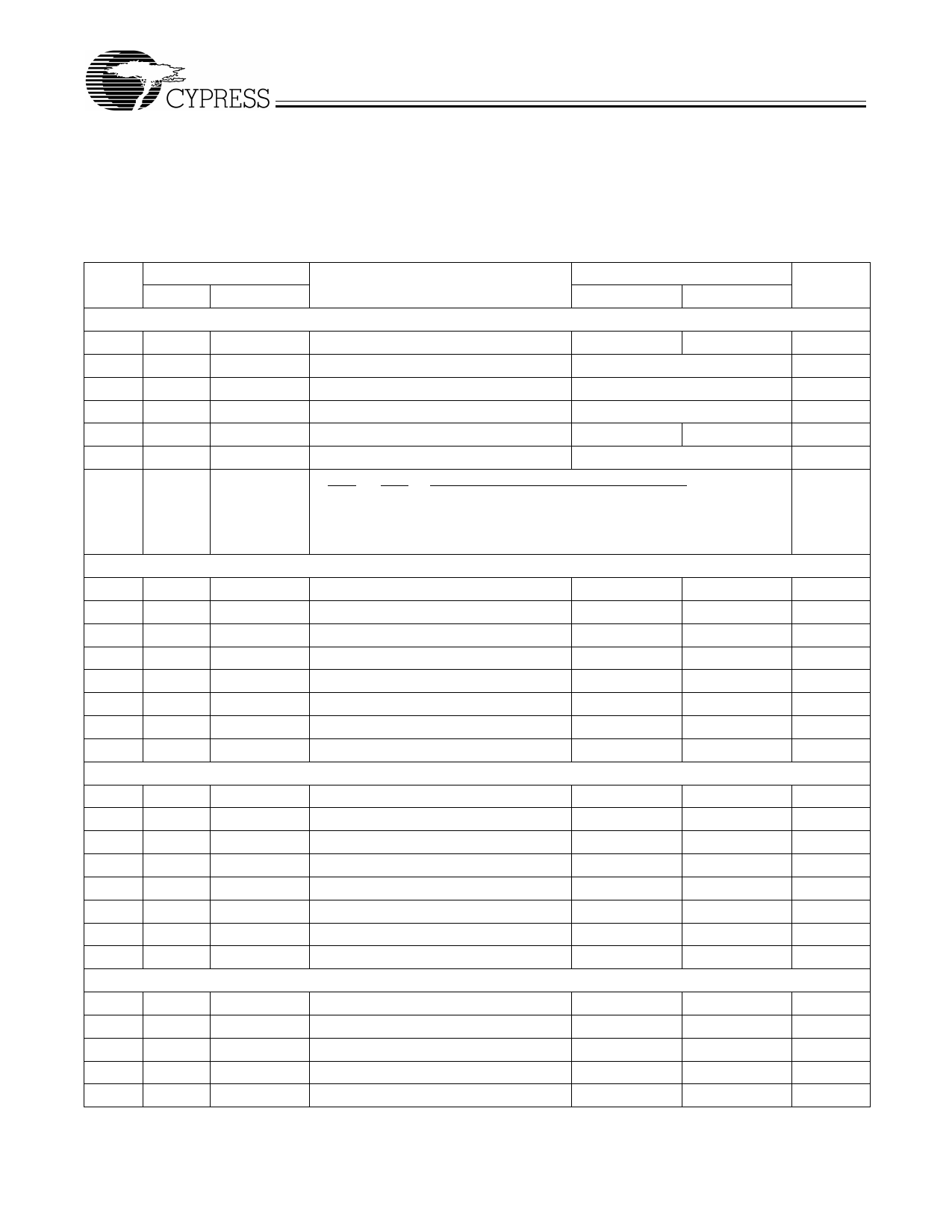
Table 5. Data Bytes 0–7 Serial Configuration Map
Affected Pin
Bit Control
Bit(s) Pin No. Pin Name
Control Function
0
1
Data Byte 0
7
--
--
(Reserved)
--
--
6
--
--
SEL_2
See Table 6
5
--
--
SEL_1
See Table 6
4
--
--
SEL_0
See Table 6
3
--
--
Hardware/Software Frequency Select
Hardware
Software
2
--
--
SEL3
See Table 6
1–0
--
--
Bit 1 Bit 0 Function (See Table 7 for function details)
0
0 Spread Spectrum Off (default)
0
1 (Reserved)
1
0 Spread Spectrum On
1
1 All Outputs Three-stated
Data Byte 1
7
--
--
(Reserved)
--
--
6
--
--
(Reserved)
--
--
5
--
--
(Reserved)
--
--
4
--
--
(Reserved)
--
--
3
40
SDRAM_F Clock Output Disable
Low
Active
2
--
--
(Reserved)
--
--
1
43
CPU1
Clock Output Disable
Low
Active
0
44
CPU_F Clock Output Disable
Low
Active
Data Byte 2
7
--
--
(Reserved)
--
--
6
7
PCI_F Clock Output Disable
Low
Active
5
--
--
(Reserved)
--
--
4
13
PCI5
Clock Output Disable
Low
Active
3
12
PCI4
Clock Output Disable
Low
Active
2
11
PCI3
Clock Output Disable
Low
Active
1
10
PCI2
Clock Output Disable
Low
Active
0
8
PCI1
Clock Output Disable
Low
Active
Data Byte 3
7
--
--
(Reserved)
--
--
6
--
--
(Reserved)
--
--
5
26
48MHz Clock Output Disable
Low
Active
4
25
24MHz Clock Output Disable
Low
Active
3
--
--
(Reserved)
--
--
Default
0
0
0
0
0
0
00
0
0
0
0
1
0
1
1
0
1
0
1
1
1
1
1
0
0
1
1
0
6
Share Link: 