W199 Просмотр технического описания (PDF) - Cypress Semiconductor
Номер в каталоге
Компоненты Описание
Список матч
W199 Datasheet PDF : 14 Pages
| |||
PRELIMINARY
W199
Overview
The W199 was developed as a single-chip device to meet the
clocking needs of the VIA Apollo Pro-133 core logic chip set.
In addition to the typical outputs provided by standard
100-MHz FTGs, the W199 adds a thirteenth output buffer, sup-
porting SDRAM DIMM modules in conjunction with the
chipset.
Cypress’s proprietary spread spectrum frequency synthesis
technique is a feature of the CPU and PCI outputs. When en-
abled, this feature reduces the peak EMI measurements of not
only the output signals and their harmonics, but also of any
other clock signals that are properly synchronized to them.
Functional Description
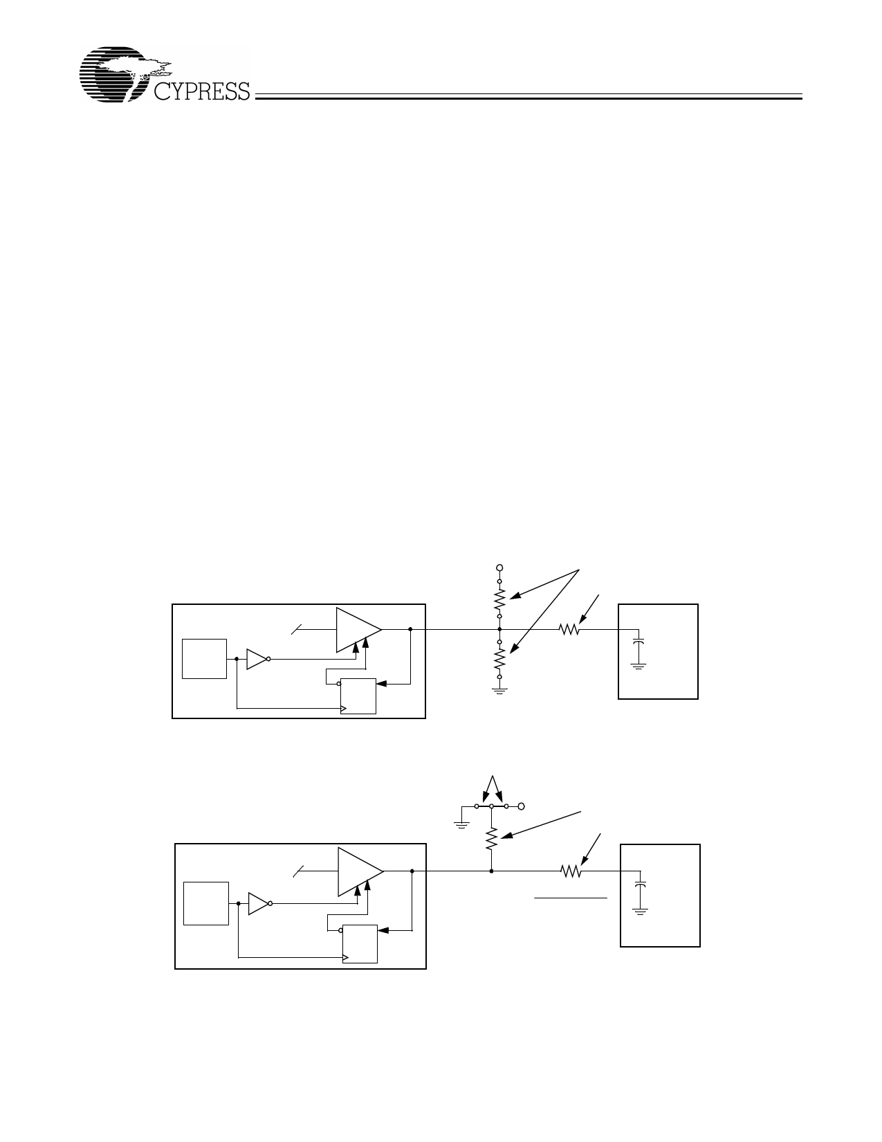
I/O Pin Operation
Pins 7, 8, 25, 26, are 46 are dual-purpose l/O pins. Upon pow-
er-up these pins act as logic inputs, allowing the determination
of assigned device functions. A short time after power-up, the
logic state of each pin is latched and the pins become clock
outputs. This feature reduces device pin count by combining
clock outputs with input select pins.
An external 10-kΩ “strapping” resistor is connected between
the l/O pin and ground or VDD. Connection to ground sets a
latch to “0,” connection to VDD sets a latch to “1.” Figure 1 and
Figure 2 show two suggested methods for strapping resistor
connections.
Upon W199 power-up, the first 2 ms of operation is used for
input logic selection. During this period, the five I/O pins (7, 8,
25, 26, 46) are three-stated, allowing the output strapping re-
sistor on the l/O pins to pull the pins and their associated ca-
pacitive clock load to either a logic HIGH or LOW state. At the
end of the 2-ms period, the established logic “0” or “1” condi-
tion of the l/O pin is latched. Next the output buffer is enabled,
converting the l/O pins into operating clock outputs. The 2-ms
timer starts when VDD reaches 2.0V. The input bits can only
be reset by turning VDD off and then back on again.
It should be noted that the strapping resistors have no signifi-
cant effect on clock output signal integrity. The drive imped-
ance of clock outputs is <40Ω (nominal), which is minimally
affected by the 10-kΩ strap to ground or VDD. As with the se-
ries termination resistor, the output strapping resistor should
be placed as close to the l/O pin as possible in order to keep
the interconnecting trace short. The trace from the resistor to
ground or VDD should be kept less than two inches in length to
minimize system noise coupling during input logic sampling.
When the clock outputs are enabled following the 2-ms input
period, the corresponding specified output frequency is deliv-
ered on the pin, assuming that VDD has stabilized. If VDD has
not yet reached full value, output frequency initially may be
below target but will increase to target once VDD voltage has
stabilized. In either case, a short output clock cycle may be
produced from the CPU clock outputs when the outputs are
enabled.
W199
Power-on
Reset
Timer
VDD
Output
Buffer
Output Three-state Hold
Output
Low
QD
Data
Latch
10 kΩ
(Load Option 1)
10 kΩ
(Load Option 0)
Output Strapping R esistor
Series Term ination Resistor
Clock Load
Figure 1. Input Logic Selection Through Resistor Load Option
Jumper Options
W199
Power-on
Reset
Timer
Output
Buffer
Output Three-state Hold
Output
Low
QD
D a ta
Latch
10 kΩ
VDD
Output Strapping Resistor
Series Termination Resistor
R
Clock Load
Resistor Value R
Figure 2. Input Logic Selection Through Jumper Option
3
Share Link: 